ZHCSMW2B December 2021 – December 2022 LM5123-Q1
PRODUCTION DATA
- 1 特性
- 2 应用
- 3 说明
- 4 Revision History
- 5 说明(续)
- 6 Pin Configuration and Functions
- 7 Specifications
-
8 Detailed Description
- 8.1 Overview
- 8.2 Functional Block Diagram
- 8.3
Feature Description
- 8.3.1 Device Enable/Disable (EN, VH Pin)
- 8.3.2 High Voltage VCC Regulator (BIAS, VCC Pin)
- 8.3.3 Light Load Switching Mode Selection (MODE Pin)
- 8.3.4 VOUT Range Selection (RANGE Pin)
- 8.3.5 Line Undervoltage Lockout (UVLO Pin)
- 8.3.6 Fast Restart using VCC HOLD (VH Pin)
- 8.3.7 Adjustable Output Regulation Target (VOUT, TRK, VREF Pin)
- 8.3.8 Overvoltage Protection (VOUT Pin)
- 8.3.9 Power Good Indicator (PGOOD Pin)
- 8.3.10 Dynamically Programmable Switching Frequency (RT)
- 8.3.11 External Clock Synchronization (SYNC Pin)
- 8.3.12 Programmable Spread Spectrum (DITHER Pin)
- 8.3.13 Programmable Soft Start (SS Pin)
- 8.3.14 Wide Bandwidth Transconductance Error Amplifier and PWM (TRK, COMP Pin)
- 8.3.15 Current Sensing and Slope Compensation (CSP, CSN Pin)
- 8.3.16 Constant Peak Current Limit (CSP, CSN Pin)
- 8.3.17 Maximum Duty Cycle and Minimum Controllable On-Time Limits
- 8.3.18 Deep Sleep Mode and Bypass Operation (HO, CP Pin)
- 8.3.19 MOSFET Drivers, Integrated Boot Diode, and Hiccup Mode Fault Protection (LO, HO, HB Pin)
- 8.3.20 Thermal Shutdown Protection
- 8.4 Device Functional Modes
- 9 Application and Implementation
- 10Power Supply Recommendations
- 11Layout
- 12Device and Documentation Support
- 13Mechanical, Packaging, and Orderable Information
8.4.2.4 Skip Mode
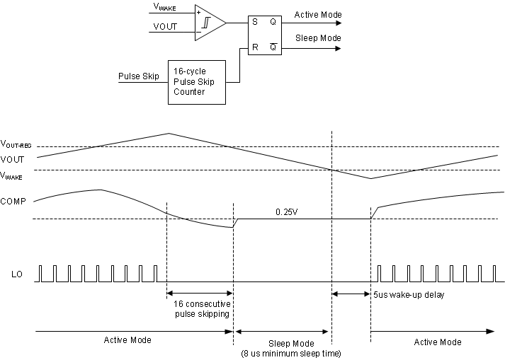
When skip mode is selected as the light load switching mode, the device enters sleep mode when the pulse skip counter detects 16 consecutive cycles of pulse skipping in the active mode, and re-enters the active mode if VOUT falls down below VWAKE.
The light load efficiency can be increased by entering sleep mode more frequently and staying in sleep mode longer. In skip mode and when SS is greater than 1.5 V, the device works in the diode emulation, but the minimum peak current is limited to 10 mV/RS once the low-side driver turns on. By limiting the minimum peak current, the boost converter is able to supply more current than what is required when switching, and enters sleep mode more frequently and stays longer in the sleep mode.
 Figure 8-23 Skip Mode Operation
When skip mode is selected as the light load switching mode, LM should be selected for the peak inductor to reach the 10m-V minimum peak current limit before LO turns off by DMAX at the minimum VSUPPLY.