ZHCSLQ5D October   2007  – August 2020 LM5067

PRODUCTION DATA  

  1. 特性
  2. 应用
  3. 说明
  4. Revision History
  5. Device Comparison
  6. Pin Configuration and Functions
    1.     Pin Functions
  7. Specifications
    1. 7.1 Absolute Maximum Ratings
    2. 7.2 ESD Ratings
    3. 7.3 Recommended Operating Conditions
    4. 7.4 Thermal Information
    5. 7.5 Electrical Characteristics
    6. 7.6 Switching Characteristics
    7. 7.7 Typical Characteristics
  8. Detailed Description
    1. 8.1 Overview
    2. 8.2 Functional Block Diagram
    3. 8.3 Feature Description
      1. 8.3.1 Power Up Sequence
      2. 8.3.2 Gate Control
      3. 8.3.3 Current Limit
      4. 8.3.4 Circuit Breaker
      5. 8.3.5 Power Limit
      6. 8.3.6 Fault Timer and Restart
      7. 8.3.7 Undervoltage Lock-Out (UVLO)
      8. 8.3.8 Overvoltage Lock-Out (OVLO)
      9. 8.3.9 Power Good Pin
    4. 8.4 Device Functional Modes
      1. 8.4.1 Shutdown / Enable Control
  9. Application and Implementation
    1. 9.1 Application Information
    2. 9.2 Typical Application
      1. 9.2.1 Design Requirements
      2. 9.2.2 Detailed Design Procedure
        1. 9.2.2.1  RIN, CIN
        2. 9.2.2.2  Current Limit, RS
        3. 9.2.2.3  Power Limit Threshold
        4. 9.2.2.4  Turn-On Time
          1. 9.2.2.4.1 Turn-on With Current Limit Only
          2. 9.2.2.4.2 Turn-on With Power Limit and Current Limit
        5. 9.2.2.5  MOSFET Selection
        6. 9.2.2.6  Timer Capacitor, CT
          1. 9.2.2.6.1 Insertion Delay
          2. 9.2.2.6.2 Fault Timeout Period
          3. 9.2.2.6.3 Restart Timing
        7. 9.2.2.7  UVLO, OVLO
          1. 9.2.2.7.1 Option A:
          2. 9.2.2.7.2 Option B:
          3. 9.2.2.7.3 Option C:
          4. 9.2.2.7.4 Option D:
        8. 9.2.2.8  Thermal Considerations
        9. 9.2.2.9  System Considerations
          1. 9.2.2.9.1 System Considerations During Surge Events
        10. 9.2.2.10 Power Good Pin
      3. 9.2.3 Application Curves
  10. 10Power Supply Recommendations
    1. 10.1 Operating Voltage
  11. 11Layout
    1. 11.1 Layout Guidelines
    2. 11.2 Layout Example
  12. 12Device and Documentation Support
    1. 12.1 Trademarks
    2. 12.2 静电放电警告
    3. 12.3 术语表
  13. 13Mechanical, Packaging, and Orderable Information

封装选项

机械数据 (封装 | 引脚)
散热焊盘机械数据 (封装 | 引脚)
订购信息
Turn-on With Power Limit and Current Limit

The power dissipation limit in Q1 (PFET(LIM)) is defined by the resistor at the PWR pin, and the current sense resistor RS. See Power Limit Threshold. If the current limit threshold (ILIM) is higher than the current defined by the power limit threshold at maximum VDS (PFET(LIM)/VSYS) the circuit operates initially in power limit mode when the VDS of Q1 is high, and then transitions to current limit mode as the current increases to ILIM as VDS decreases. See Figure 9-5b. Assuming the load (RL) is not connected during turn-on, the time for the output voltage to reach its final value is approximately equal to:

Equation 6. GUID-B4827ECF-3BA1-4F2C-B766-3491B179FCF8-low.gif

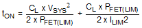
For example, if VSYS = –48 V, CL = 1000 µF, ILIM = 1 A, and PFET(LIM) = 20 W, tON calculates to ≊ 68 ms, and the initial current level (IP) is approximately 0.42A.

Note:

The Fault Timeout Period must be set longer than tON

GUID-6FA7B7A2-272F-4B21-842C-342D9F48283B-low.gifFigure 9-5 MOSFET Power Up Waveforms