ZHCSLQ5D October 2007 – August 2020 LM5067
PRODUCTION DATA
- 1 特性
- 2 应用
- 3 说明
- 4 Revision History
- 5 Device Comparison
- 6 Pin Configuration and Functions
- 7 Specifications
- 8 Detailed Description
-
9 Application and Implementation
- 9.1 Application Information
- 9.2
Typical Application
- 9.2.1 Design Requirements
- 9.2.2 Detailed Design Procedure
- 9.2.3 Application Curves
- 10Power Supply Recommendations
- 11Layout
- 12Device and Documentation Support
- 13Mechanical, Packaging, and Orderable Information
9.2.2.2 Current Limit, RS
The LM5067 monitors the current in the external MOSFET (Q1) by measuring the voltage across the sense resistor (RS), connected from SENSE to VEE. The required resistor value is calculated from:

where
- ILIM is the desired current limit threshold
When the voltage across RS reaches 50 mV, the current limit circuit modulates the gate of Q1 to regulate the current at ILIM. While the current limiting circuit is active, the fault timer is active as described in the Fault Timer and Restart section. For proper operation, RS must be no larger than 100 mΩ.
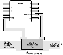
While the maximum load current in normal operation can be used to determine the required power rating for resistor RS, basing it on the current limit value provides a more reliable design since the circuit can operate near the current limit threshold continuously. The resistor’s surge capability must also be considered since the circuit breaker threshold is approximately twice the current limit threshold. Connections from RS to the LM5067 should be made using Kelvin techniques. In the suggested layout of Figure 9-2 the small pads at the upper corners of the sense resistor connect only to the sense resistor terminals, and not to the traces carrying the high current. With this technique, only the voltage across the sense resistor is applied to VEE and SENSE, eliminating the voltage drop across the high current solder connections.
 Figure 9-2 Sense Resistor Connections