ZHCSLQ5D October 2007 – August 2020 LM5067
PRODUCTION DATA
- 1 特性
- 2 应用
- 3 说明
- 4 Revision History
- 5 Device Comparison
- 6 Pin Configuration and Functions
- 7 Specifications
- 8 Detailed Description
-
9 Application and Implementation
- 9.1 Application Information
- 9.2
Typical Application
- 9.2.1 Design Requirements
- 9.2.2 Detailed Design Procedure
- 9.2.3 Application Curves
- 10Power Supply Recommendations
- 11Layout
- 12Device and Documentation Support
- 13Mechanical, Packaging, and Orderable Information
9.2.2.4.1 Turn-on With Current Limit Only
If the current limit threshold is less than the current defined by the power limit threshold at maximum VDS the circuit operates only at the current limit threshold during turn-on. Referring to Figure 9-5a, as the drain current reaches ILIM, the gate-to-source voltage is controlled at VGSL to maintain the current at ILIM. As the output voltage reaches its final value (VDS ≊ 0 V) the drain current reduces to the value defined by the load, and the gate is charged to approximately 13 V (VGATE). The time for the OUT pin voltage to transition from zero volts to VSYS is equal to:

where
- CL is the load capacitance
For example, if VSYS = –48 V, CL = 1000 µF, and ILIM = 1 A, tON calculates to 48 ms. The maximum instantaneous power dissipated in the MOSFET is 48W. This calculation assumes the time from t1 to t2 in Figure 9-5a is small compared to tON, and the load does not draw any current until after the output voltage has reached its final value, and PGD switches high (Figure 9-3).
 Figure 9-3 No Load Current During Turn-on
If the load draws current during the turn-on sequence (Figure 9-4), the turn-on time is longer than the above calculation, and is approximately equal to:
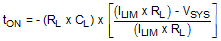
where
- RL is the load resistance and VSYS is the absolute value of the system input voltage
The Fault Timeout Period must be set longer than tON to prevent a fault shutdown before the turn-on sequence is complete.
 Figure 9-4 Load Draws Current During Turn-On