ZHCSLQ5D October   2007  – August 2020 LM5067

PRODUCTION DATA  

  1. 特性
  2. 应用
  3. 说明
  4. Revision History
  5. Device Comparison
  6. Pin Configuration and Functions
    1.     Pin Functions
  7. Specifications
    1. 7.1 Absolute Maximum Ratings
    2. 7.2 ESD Ratings
    3. 7.3 Recommended Operating Conditions
    4. 7.4 Thermal Information
    5. 7.5 Electrical Characteristics
    6. 7.6 Switching Characteristics
    7. 7.7 Typical Characteristics
  8. Detailed Description
    1. 8.1 Overview
    2. 8.2 Functional Block Diagram
    3. 8.3 Feature Description
      1. 8.3.1 Power Up Sequence
      2. 8.3.2 Gate Control
      3. 8.3.3 Current Limit
      4. 8.3.4 Circuit Breaker
      5. 8.3.5 Power Limit
      6. 8.3.6 Fault Timer and Restart
      7. 8.3.7 Undervoltage Lock-Out (UVLO)
      8. 8.3.8 Overvoltage Lock-Out (OVLO)
      9. 8.3.9 Power Good Pin
    4. 8.4 Device Functional Modes
      1. 8.4.1 Shutdown / Enable Control
  9. Application and Implementation
    1. 9.1 Application Information
    2. 9.2 Typical Application
      1. 9.2.1 Design Requirements
      2. 9.2.2 Detailed Design Procedure
        1. 9.2.2.1  RIN, CIN
        2. 9.2.2.2  Current Limit, RS
        3. 9.2.2.3  Power Limit Threshold
        4. 9.2.2.4  Turn-On Time
          1. 9.2.2.4.1 Turn-on With Current Limit Only
          2. 9.2.2.4.2 Turn-on With Power Limit and Current Limit
        5. 9.2.2.5  MOSFET Selection
        6. 9.2.2.6  Timer Capacitor, CT
          1. 9.2.2.6.1 Insertion Delay
          2. 9.2.2.6.2 Fault Timeout Period
          3. 9.2.2.6.3 Restart Timing
        7. 9.2.2.7  UVLO, OVLO
          1. 9.2.2.7.1 Option A:
          2. 9.2.2.7.2 Option B:
          3. 9.2.2.7.3 Option C:
          4. 9.2.2.7.4 Option D:
        8. 9.2.2.8  Thermal Considerations
        9. 9.2.2.9  System Considerations
          1. 9.2.2.9.1 System Considerations During Surge Events
        10. 9.2.2.10 Power Good Pin
      3. 9.2.3 Application Curves
  10. 10Power Supply Recommendations
    1. 10.1 Operating Voltage
  11. 11Layout
    1. 11.1 Layout Guidelines
    2. 11.2 Layout Example
  12. 12Device and Documentation Support
    1. 12.1 Trademarks
    2. 12.2 静电放电警告
    3. 12.3 术语表
  13. 13Mechanical, Packaging, and Orderable Information

封装选项

机械数据 (封装 | 引脚)
散热焊盘机械数据 (封装 | 引脚)
订购信息
Option B:

If all four thresholds must be accurately defined, the configuration in Figure 9-7 can be used.

GUID-9BC63FD7-F980-4C87-8865-C678B3EA1C30-low.gifFigure 9-7 Programming the Four Thresholds

The four resistor values are calculated as follows:

  • Determine the upper UVLO threshold (VUVH) to enable Q1, and the lower UVLO threshold (VUVL) to disable Q1.
    Equation 14. GUID-CD6ECF70-735F-48E3-A732-D030C286FF5C-low.gif
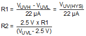
  • Determine the upper OVLO threshold (VOVH) to disable Q1, and the lower OVLO threshold (VOVL) to enable Q1.
    Equation 15. GUID-DDC389B0-049F-4492-B337-5AAA168756A5-low.gif

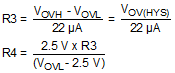
As an example, assume the application requires the following thresholds: VUVH = –22 V, VUVL = –17 V, VOVH = –60 V, and VOVL = –58 V. Therefore VUV(HYS) = 5 V, and VOV(HYS) = 2 V. The resistor values are:

R1 = 227 kΩ, R2 = 39.1 kΩ

R3 = 90.9 kΩ, R4 = 3.95 kΩ

Where the R1-R4 resistor values are known, the threshold voltages and hysteresis are calculated from the following:

Equation 16. GUID-59E731CE-AA5E-4304-BFA1-70FFDCF91EDE-low.gif
Note:

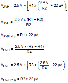
Ensure the voltages at the UVLO and OVLO pins do not exceed the Absolute Maximum ratings for those pins when the system voltage is at maximum.