ZHCSIQ5A September 2018 – August 2021 LM34936
PRODUCTION DATA
- 1 特性
- 2 应用
- 3 说明
- 4 Revision History
- 5 Pin Configuration and Functions
- 6 Specifications
-
7 Detailed Description
- 7.1 Overview
- 7.2 Functional Block Diagram
- 7.3
Feature Description
- 7.3.1 Fixed Frequency Valley/Peak Current Mode Control with Slope Compensation
- 7.3.2 VCC Regulator and Optional BIAS Input
- 7.3.3 Enable/UVLO
- 7.3.4 Soft-Start
- 7.3.5 Overcurrent Protection
- 7.3.6 Average Input/Output Current Limiting
- 7.3.7 Operation Above 28-V Input
- 7.3.8 CCM Operation
- 7.3.9 Frequency and Synchronization (RT/SYNC)
- 7.3.10 Frequency Dithering
- 7.3.11 Output Overvoltage Protection (OVP)
- 7.3.12 Power Good (PGOOD)
- 7.3.13 Gm Error Amplifier
- 7.3.14 Integrated Gate Drivers
- 7.3.15 Thermal Shutdown
- 7.4 Device Functional Modes
-
8 Application and Implementation
- 8.1 Application Information
- 8.2
Typical Application
- 8.2.1 Design Requirements
- 8.2.2
Detailed Design Procedure
- 8.2.2.1 Custom Design with WEBENCH Tools
- 8.2.2.2 Frequency
- 8.2.2.3 VOUT
- 8.2.2.4 Inductor Selection
- 8.2.2.5 Output Capacitor
- 8.2.2.6 Input Capacitor
- 8.2.2.7 Sense Resistor (RSENSE)
- 8.2.2.8 Slope Compensation
- 8.2.2.9 UVLO
- 8.2.2.10 Soft-Start Capacitor
- 8.2.2.11 Dither Capacitor
- 8.2.2.12 MOSFETs QH1 and QL1
- 8.2.2.13 MOSFETs QH2 and QL2
- 8.2.2.14 Frequency Compensation
- 8.2.3 Application Curves
- 9 Power Supply Recommendations
- 10Layout
- 11Device and Documentation Support
- 12Mechanical, Packaging, and Orderable Information
8.2.2.4 Inductor Selection
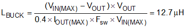
The inductor selection is based on consideration of both buck and boost modes of operation. For the buck mode, inductor selection is based on limiting the peak to peak current ripple ΔIL to ~40% of the maximum inductor current at the maximum input voltage. The target inductance for the buck mode is:
For the boost mode, the inductor selection is based on limiting the peak to peak current ripple ΔIL to ~30% of the maximum inductor current at the minimum input voltage. The target inductance for the boost mode is:
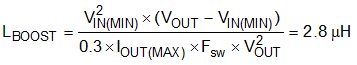
In this particular application, the buck inductance is larger. Choosing a larger inductance reduces the ripple current but also increases the size of the inductor. A larger inductor also reduces the achievable bandwidth of the converter by moving the right half plane zero to lower frequencies. Therefore a judicious compromise should be made based on the application requirements. For this design a 4.7-µH inductor is selected. With this inductor selection, the inductor current ripple is 5.1 A, 4.3 A, and 2.1 A, at VIN of 30 V, 24 V, and 6 V respectively.
The maximum average inductor current occurs at the minimum input voltage and maximum load current:
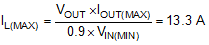
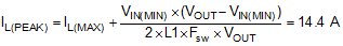
where a 90% efficiency is assumed. The peak inductor current occurs at minimum input voltage and is given by:
To ensure sufficient output current, the current limit threshold must be set to allow the maximum load current in boost operation. The inductor peak current during overload depends on the current limit resistor RSENSE (refer to the sub-section on selecting RSENSE). The peak inductor current in current limit when in boost mode is given by:
The peak inductor current in current limit when in buck mode happens at high input voltage and is given by:
The peak inductor current in current limit is 15 A and 16.5 A in boost mode and buck mode respectively. The inductor should be selected to handle this current.