ZHCSIQ5A September 2018 – August 2021 LM34936
PRODUCTION DATA
- 1 特性
- 2 应用
- 3 说明
- 4 Revision History
- 5 Pin Configuration and Functions
- 6 Specifications
-
7 Detailed Description
- 7.1 Overview
- 7.2 Functional Block Diagram
- 7.3
Feature Description
- 7.3.1 Fixed Frequency Valley/Peak Current Mode Control with Slope Compensation
- 7.3.2 VCC Regulator and Optional BIAS Input
- 7.3.3 Enable/UVLO
- 7.3.4 Soft-Start
- 7.3.5 Overcurrent Protection
- 7.3.6 Average Input/Output Current Limiting
- 7.3.7 Operation Above 28-V Input
- 7.3.8 CCM Operation
- 7.3.9 Frequency and Synchronization (RT/SYNC)
- 7.3.10 Frequency Dithering
- 7.3.11 Output Overvoltage Protection (OVP)
- 7.3.12 Power Good (PGOOD)
- 7.3.13 Gm Error Amplifier
- 7.3.14 Integrated Gate Drivers
- 7.3.15 Thermal Shutdown
- 7.4 Device Functional Modes
-
8 Application and Implementation
- 8.1 Application Information
- 8.2
Typical Application
- 8.2.1 Design Requirements
- 8.2.2
Detailed Design Procedure
- 8.2.2.1 Custom Design with WEBENCH Tools
- 8.2.2.2 Frequency
- 8.2.2.3 VOUT
- 8.2.2.4 Inductor Selection
- 8.2.2.5 Output Capacitor
- 8.2.2.6 Input Capacitor
- 8.2.2.7 Sense Resistor (RSENSE)
- 8.2.2.8 Slope Compensation
- 8.2.2.9 UVLO
- 8.2.2.10 Soft-Start Capacitor
- 8.2.2.11 Dither Capacitor
- 8.2.2.12 MOSFETs QH1 and QL1
- 8.2.2.13 MOSFETs QH2 and QL2
- 8.2.2.14 Frequency Compensation
- 8.2.3 Application Curves
- 9 Power Supply Recommendations
- 10Layout
- 11Device and Documentation Support
- 12Mechanical, Packaging, and Orderable Information
7.3.13 Gm Error Amplifier
The LM34936 has a gm error amplifier for loop compensation. The gm amplifier output (COMP) range is 0.3 V to 3 V. Connect an Rc1-Cc1 compensation network between COMP and ground for type II (PI) compensation (see Figure 8-1). Another pole is usually added using Cc2 to suppress higher frequency noise and switching frequency ripple.
The COMP output voltage (VCOMP) range limits the possible VIN and IOUT range for a given design. In buck mode, the maximum VIN for which the converter can regulate the output at no load is when VCOMP reaches 0.3 V. Equation 7 gives VCOMP as a function of VIN at no load in CCM buck mode:

Where DBUCK in the equation Equation 7 is the buck duty cycle given by:

A larger L1, lower slope ripple (higher CSLOPE), smaller sense resistor (RSENSE), and higher frequency can increase the maximum VIN range for buck operation.
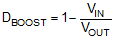
For boost mode, the minimum VIN for which the converter can regulate the output at full load is when VCOMP reaches 3 V. Equation 9 gives VCOMP as a function of VIN in boost mode:

Where DBOOST in the Equation 9 is the boost duty cycle given by:
A larger L1, lower slope ripple (higher CSLOPE), smaller sense resistor (RSENSE), and higher frequency can extend the minimum VIN range for boost operation.