ZHCSIQ5A September 2018 – August 2021 LM34936
PRODUCTION DATA
- 1 特性
- 2 应用
- 3 说明
- 4 Revision History
- 5 Pin Configuration and Functions
- 6 Specifications
-
7 Detailed Description
- 7.1 Overview
- 7.2 Functional Block Diagram
- 7.3
Feature Description
- 7.3.1 Fixed Frequency Valley/Peak Current Mode Control with Slope Compensation
- 7.3.2 VCC Regulator and Optional BIAS Input
- 7.3.3 Enable/UVLO
- 7.3.4 Soft-Start
- 7.3.5 Overcurrent Protection
- 7.3.6 Average Input/Output Current Limiting
- 7.3.7 Operation Above 28-V Input
- 7.3.8 CCM Operation
- 7.3.9 Frequency and Synchronization (RT/SYNC)
- 7.3.10 Frequency Dithering
- 7.3.11 Output Overvoltage Protection (OVP)
- 7.3.12 Power Good (PGOOD)
- 7.3.13 Gm Error Amplifier
- 7.3.14 Integrated Gate Drivers
- 7.3.15 Thermal Shutdown
- 7.4 Device Functional Modes
-
8 Application and Implementation
- 8.1 Application Information
- 8.2
Typical Application
- 8.2.1 Design Requirements
- 8.2.2
Detailed Design Procedure
- 8.2.2.1 Custom Design with WEBENCH Tools
- 8.2.2.2 Frequency
- 8.2.2.3 VOUT
- 8.2.2.4 Inductor Selection
- 8.2.2.5 Output Capacitor
- 8.2.2.6 Input Capacitor
- 8.2.2.7 Sense Resistor (RSENSE)
- 8.2.2.8 Slope Compensation
- 8.2.2.9 UVLO
- 8.2.2.10 Soft-Start Capacitor
- 8.2.2.11 Dither Capacitor
- 8.2.2.12 MOSFETs QH1 and QL1
- 8.2.2.13 MOSFETs QH2 and QL2
- 8.2.2.14 Frequency Compensation
- 8.2.3 Application Curves
- 9 Power Supply Recommendations
- 10Layout
- 11Device and Documentation Support
- 12Mechanical, Packaging, and Orderable Information
7.3.6 Average Input/Output Current Limiting
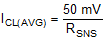
The LM34936 provides optional average current limiting capability to limit either the input or the output current of the DC/DC converter. The average current limiting circuit uses an additional current sense resistor connected in series with the input supply or output voltage of the converter. A current sense gm amplifier with inputs at the ISNS(+) and ISNS(-) pins monitors the voltage across the sense resistor and compares it with an internal 50 mV reference. If the drop across the sense resistor is greater than 50 mV, the gm amplifier gradually discharges the soft-start capacitor. When the soft-start capacitor discharges below the feedback reference voltage VREF, the output voltage of the converter decreases to limit the input or output current. The average current limiting feature can be used in applications requiring a regulated current from the input supply or into the load. The target constant current is given by Equation 4:
A filter network as shown in Figure 8-1 is often used across ISNS(+) and ISNS(-) pins to filter the ripple in the average current sense signal.
The average current loop can be disabled by shorting the ISNS(+) and ISNS(-) pins together to AGND.