ZHCSIQ5A September 2018 – August 2021 LM34936
PRODUCTION DATA
- 1 特性
- 2 应用
- 3 说明
- 4 Revision History
- 5 Pin Configuration and Functions
- 6 Specifications
-
7 Detailed Description
- 7.1 Overview
- 7.2 Functional Block Diagram
- 7.3
Feature Description
- 7.3.1 Fixed Frequency Valley/Peak Current Mode Control with Slope Compensation
- 7.3.2 VCC Regulator and Optional BIAS Input
- 7.3.3 Enable/UVLO
- 7.3.4 Soft-Start
- 7.3.5 Overcurrent Protection
- 7.3.6 Average Input/Output Current Limiting
- 7.3.7 Operation Above 28-V Input
- 7.3.8 CCM Operation
- 7.3.9 Frequency and Synchronization (RT/SYNC)
- 7.3.10 Frequency Dithering
- 7.3.11 Output Overvoltage Protection (OVP)
- 7.3.12 Power Good (PGOOD)
- 7.3.13 Gm Error Amplifier
- 7.3.14 Integrated Gate Drivers
- 7.3.15 Thermal Shutdown
- 7.4 Device Functional Modes
-
8 Application and Implementation
- 8.1 Application Information
- 8.2
Typical Application
- 8.2.1 Design Requirements
- 8.2.2
Detailed Design Procedure
- 8.2.2.1 Custom Design with WEBENCH Tools
- 8.2.2.2 Frequency
- 8.2.2.3 VOUT
- 8.2.2.4 Inductor Selection
- 8.2.2.5 Output Capacitor
- 8.2.2.6 Input Capacitor
- 8.2.2.7 Sense Resistor (RSENSE)
- 8.2.2.8 Slope Compensation
- 8.2.2.9 UVLO
- 8.2.2.10 Soft-Start Capacitor
- 8.2.2.11 Dither Capacitor
- 8.2.2.12 MOSFETs QH1 and QL1
- 8.2.2.13 MOSFETs QH2 and QL2
- 8.2.2.14 Frequency Compensation
- 8.2.3 Application Curves
- 9 Power Supply Recommendations
- 10Layout
- 11Device and Documentation Support
- 12Mechanical, Packaging, and Orderable Information
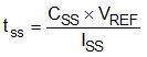
7.3.4 Soft-Start
The LM34936 soft-start time is programmed using a soft-start capacitor from the SS pin to AGND. When the converter is enabled, an internal current source (ISS) charges the soft-start capacitor. When the SS pin voltage is below the feedback reference voltage VREF, the soft-start pin controls the regulated FB voltage. Once SS exceeds VREF, the soft-start interval is complete and the error amplifier is referenced to VREF. The soft-start time is given by Equation 3:
The soft-start capacitor is internally discharged when the converter is disabled because of EN/UVLO falling below the operating threshold or VCC falling below the VCC UV threshold. The soft-start pin is also discharged when the converter is in hiccup mode current limiting or in thermal shutdown. When average input or output current limiting is active, the soft-start capacitor is discharged by the constant current loop transconductance (gm) amplifier to limit either input or output current.