ZHCSIQ5A September 2018 – August 2021 LM34936
PRODUCTION DATA
- 1 特性
- 2 应用
- 3 说明
- 4 Revision History
- 5 Pin Configuration and Functions
- 6 Specifications
-
7 Detailed Description
- 7.1 Overview
- 7.2 Functional Block Diagram
- 7.3
Feature Description
- 7.3.1 Fixed Frequency Valley/Peak Current Mode Control with Slope Compensation
- 7.3.2 VCC Regulator and Optional BIAS Input
- 7.3.3 Enable/UVLO
- 7.3.4 Soft-Start
- 7.3.5 Overcurrent Protection
- 7.3.6 Average Input/Output Current Limiting
- 7.3.7 Operation Above 28-V Input
- 7.3.8 CCM Operation
- 7.3.9 Frequency and Synchronization (RT/SYNC)
- 7.3.10 Frequency Dithering
- 7.3.11 Output Overvoltage Protection (OVP)
- 7.3.12 Power Good (PGOOD)
- 7.3.13 Gm Error Amplifier
- 7.3.14 Integrated Gate Drivers
- 7.3.15 Thermal Shutdown
- 7.4 Device Functional Modes
-
8 Application and Implementation
- 8.1 Application Information
- 8.2
Typical Application
- 8.2.1 Design Requirements
- 8.2.2
Detailed Design Procedure
- 8.2.2.1 Custom Design with WEBENCH Tools
- 8.2.2.2 Frequency
- 8.2.2.3 VOUT
- 8.2.2.4 Inductor Selection
- 8.2.2.5 Output Capacitor
- 8.2.2.6 Input Capacitor
- 8.2.2.7 Sense Resistor (RSENSE)
- 8.2.2.8 Slope Compensation
- 8.2.2.9 UVLO
- 8.2.2.10 Soft-Start Capacitor
- 8.2.2.11 Dither Capacitor
- 8.2.2.12 MOSFETs QH1 and QL1
- 8.2.2.13 MOSFETs QH2 and QL2
- 8.2.2.14 Frequency Compensation
- 8.2.3 Application Curves
- 9 Power Supply Recommendations
- 10Layout
- 11Device and Documentation Support
- 12Mechanical, Packaging, and Orderable Information
8.2.2.14 Frequency Compensation
This section presents the control loop compensation design procedure for the LM34936 buck-boost controller. The LM34936 operates mainly in buck or boost modes, separated by a transition region, and therefore the control loop design is done for both buck and boost operating modes. Then a final selection of compensation is made based on the mode that is more restrictive from a loop stability point of view. Typically for a converter designed to go deep into both buck and boost operating regions, the boost compensation design is more restrictive due to the presence of a right half plane zero (RHPZ) in the boost mode.
The boost power stage output pole location is given by:
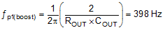
where ROUT = 2 Ω corresponds to the maximum load of 6 A.
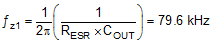
The boost power stage ESR zero location is given by:
The boost power stage RHP zero location is given by:
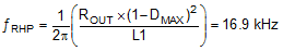
where DMAX is the maximum duty cycle at the minimum VIN.
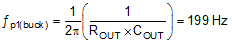
The buck power stage output pole location is given by:
The buck power stage ESR zero location is the same as the boost power stage ESR zero.
It is clear from Equation 40 that RHP zero is the main factor limiting the achievable bandwidth. For a robust design the crossover frequency should be less than 1/3 of the RHP zero frequency. Given the position of the RHP zero, a reasonable target bandwidth in boost operation is around 4 kHz:

For some power stages, the boost RHP zero might not be as restrictive. This happens when the boost maximum duty cycle (DMAX) is small, or when a really small inductor is used. In those cases, compare the limits posed by the RHP zero (fRHP/3) with 1/20 of the switching frequency and use the smaller of the two values as the achievable bandwidth.
The compensation zero can be placed at 1.5 times the boost output pole frequency. Keep in mind that this locates the zero at 3 times the buck output pole frequency which results in approximately 30 degrees of phase loss before crossover of the buck loop and 15 degrees of phase loss at intermediate frequencies for the boost loop:

If the crossover frequency is well below the RHP zero and the compensation zero is placed well below the crossover, the compensation gain resistor Rc1 is calculated using the approximation:
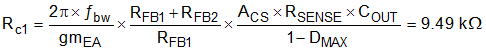
where DMAX is the maximum duty cycle at the minimum VIN in boost mode and ACS is the current sense amplifier gain. The compensation capacitor Cc1 is then calculated from:
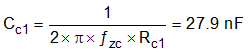
The standard values of compensation components are selected to be Rc1 = 10 kΩ and Cc1 = 33 nF.
A high frequency pole (fpc2) is placed using a capacitor (Cc2) in parallel with Rc1 and Cc1. Set the frequency of this pole at 7 to 10 times of fbw to provide attenuation of switching ripple and noise on COMP while avoiding excessive phase loss at the crossover frequency. For a target fpc2 = 28 kHz, Cc2 is calculated using this equation:
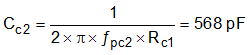
Select a standard value of 560 pF for Cc2. These values provide a good starting point for the compensation design. Each design should be tuned in the lab to achieve the desired balance between stability margin across the operating range and transient response time.