ZHCSQP4K December 2008 – June 2022 LM25088 , LM25088-Q1
PRODUCTION DATA
- 1 特性
- 2 应用
- 3 说明
- 4 Revision History
- 5 Pin Configuration and Functions
- 6 Specifications
-
7 Detailed Description
- 7.1 Overview
- 7.2 Functional Block Diagram
- 7.3
Feature Description
- 7.3.1 High Voltage Low-Dropout Regulator
- 7.3.2 Line Undervoltage Detector
- 7.3.3 Oscillator and Sync Capability
- 7.3.4 Error Amplifier and PWM Comparator
- 7.3.5 Ramp Generator
- 7.3.6 Dropout Voltage Reduction
- 7.3.7 Frequency Dithering (LM25088-1 Only)
- 7.3.8 Cycle-by-Cycle Current Limit
- 7.3.9 Overload Protection Timer (LM25088-2 Only)
- 7.3.10 Soft Start
- 7.3.11 HG Output
- 7.3.12 Thermal Protection
- 7.4 Device Functional Modes
-
8 Application and Implementation
- 8.1 Application Information
- 8.2
Typical Application
- 8.2.1 Design Requirements
- 8.2.2
Detailed Design Procedure
- 8.2.2.1 Timing Resistor
- 8.2.2.2 Output Inductor
- 8.2.2.3 Current Sense Resistor
- 8.2.2.4 Ramp Capacitor
- 8.2.2.5 Output Capacitors
- 8.2.2.6 Input Capacitors
- 8.2.2.7 VCC Capacitor
- 8.2.2.8 Bootstrap Capacitor
- 8.2.2.9 Soft-Start Capacitor
- 8.2.2.10 Output Voltage Divider
- 8.2.2.11 UVLO Divider
- 8.2.2.12 Restart Capacitor (LM5008-2 Only)
- 8.2.2.13 MOSFET Selection
- 8.2.2.14 Diode Selection
- 8.2.2.15 Snubber Components Selection
- 8.2.2.16 Error Amplifier Compensation
- 8.2.3 Application Curves
- 9 Power Supply Recommendations
- 10Layout
- 11Device and Documentation Support
- 12Mechanical, Packaging, and Orderable Information
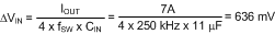
8.2.2.6 Input Capacitors
The input power supply typically has large source impedance at the switching frequency. Good quality input capacitors are necessary to limit the ripple voltage at the VIN pin while supplying most of the switch current during the on time. When the buck switch turns on, the current into the external FET steps to the valley of the inductor current waveform at turn-on, ramps up to the peak value, and then drops to zero at turn-off. The input capacitors must be selected for RMS current rating and minimum ripple voltage. A good approximation for the ripple current is IRMS > IOUT / 2.
Quality ceramic capacitors with a low ESR must be selected for the input filter. To allow for capacitor tolerances and voltage rating, five 2.2-µF, 100-V ceramic capacitors were selected. With ceramic capacitors, the input ripple voltage is triangular and peaks at 50% duty cycle. Taking into account the capacitance change with DC bias, a worst case input peak-to-peak ripple voltage can be approximated as:
When the converter is connected to an input power source, a resonant circuit is formed by the line impedance and the input capacitors. This can result in an overshoot at the VIN pin and can result in VIN exceeding its absolute maximum rating. Because of those conditions, it is recommended that either an aluminum type capacitor with an ESR or increasing CIN > 10 × LIN. While using aluminum type capacitor, take care to not exceed its maximum ripple current rating. Tantalum capacitors must be avoided at the input as they are prone to shorting.