ZHCSQP4K December 2008 – June 2022 LM25088 , LM25088-Q1
PRODUCTION DATA
- 1 特性
- 2 应用
- 3 说明
- 4 Revision History
- 5 Pin Configuration and Functions
- 6 Specifications
-
7 Detailed Description
- 7.1 Overview
- 7.2 Functional Block Diagram
- 7.3
Feature Description
- 7.3.1 High Voltage Low-Dropout Regulator
- 7.3.2 Line Undervoltage Detector
- 7.3.3 Oscillator and Sync Capability
- 7.3.4 Error Amplifier and PWM Comparator
- 7.3.5 Ramp Generator
- 7.3.6 Dropout Voltage Reduction
- 7.3.7 Frequency Dithering (LM25088-1 Only)
- 7.3.8 Cycle-by-Cycle Current Limit
- 7.3.9 Overload Protection Timer (LM25088-2 Only)
- 7.3.10 Soft Start
- 7.3.11 HG Output
- 7.3.12 Thermal Protection
- 7.4 Device Functional Modes
-
8 Application and Implementation
- 8.1 Application Information
- 8.2
Typical Application
- 8.2.1 Design Requirements
- 8.2.2
Detailed Design Procedure
- 8.2.2.1 Timing Resistor
- 8.2.2.2 Output Inductor
- 8.2.2.3 Current Sense Resistor
- 8.2.2.4 Ramp Capacitor
- 8.2.2.5 Output Capacitors
- 8.2.2.6 Input Capacitors
- 8.2.2.7 VCC Capacitor
- 8.2.2.8 Bootstrap Capacitor
- 8.2.2.9 Soft-Start Capacitor
- 8.2.2.10 Output Voltage Divider
- 8.2.2.11 UVLO Divider
- 8.2.2.12 Restart Capacitor (LM5008-2 Only)
- 8.2.2.13 MOSFET Selection
- 8.2.2.14 Diode Selection
- 8.2.2.15 Snubber Components Selection
- 8.2.2.16 Error Amplifier Compensation
- 8.2.3 Application Curves
- 9 Power Supply Recommendations
- 10Layout
- 11Device and Documentation Support
- 12Mechanical, Packaging, and Orderable Information
7.3.8 Cycle-by-Cycle Current Limit
The LM25088 contains a current limit feature that protects the circuit from extended overcurrent conditions. The emulated current signal is directly proportional to the buck switch current and is applied to the current limit comparator. If the emulated current exceeds 1.2 V, the PWM cycle is terminated. The peak inductor current required to trigger the current limit comparator is given by:
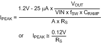
where
- A = 10 V/V is the current sense amplifier gain.
- CRAMP is the ramp capacitor.
- RS is the sense resistor.
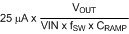 is the voltage ramp
added for slope compensation.
is the voltage ramp
added for slope compensation.- 1.2 V is the reference of the current limit comparator.
Since the current that charges the RAMP capacitor is proportional to VIN – VOUT, if the output is suddenly shorted, the VOUT term is zero and the RAMP charging current increases. The increased RAMP charging current immediately reduces the PWM duty cycle. The LM25088 also includes a buck switch protection scheme. A dedicated comparator monitors the drain-to-source voltage of the buck FET when it is turned ON. If VDS exceeds 1.5 V, the comparator turns of the buck FET immediately. This feature helps protect the buck FET in catastrophic conditions, such as a sudden saturation of the inductor.