ZHCSQP4K December 2008 – June 2022 LM25088 , LM25088-Q1
PRODUCTION DATA
- 1 特性
- 2 应用
- 3 说明
- 4 Revision History
- 5 Pin Configuration and Functions
- 6 Specifications
-
7 Detailed Description
- 7.1 Overview
- 7.2 Functional Block Diagram
- 7.3
Feature Description
- 7.3.1 High Voltage Low-Dropout Regulator
- 7.3.2 Line Undervoltage Detector
- 7.3.3 Oscillator and Sync Capability
- 7.3.4 Error Amplifier and PWM Comparator
- 7.3.5 Ramp Generator
- 7.3.6 Dropout Voltage Reduction
- 7.3.7 Frequency Dithering (LM25088-1 Only)
- 7.3.8 Cycle-by-Cycle Current Limit
- 7.3.9 Overload Protection Timer (LM25088-2 Only)
- 7.3.10 Soft Start
- 7.3.11 HG Output
- 7.3.12 Thermal Protection
- 7.4 Device Functional Modes
-
8 Application and Implementation
- 8.1 Application Information
- 8.2
Typical Application
- 8.2.1 Design Requirements
- 8.2.2
Detailed Design Procedure
- 8.2.2.1 Timing Resistor
- 8.2.2.2 Output Inductor
- 8.2.2.3 Current Sense Resistor
- 8.2.2.4 Ramp Capacitor
- 8.2.2.5 Output Capacitors
- 8.2.2.6 Input Capacitors
- 8.2.2.7 VCC Capacitor
- 8.2.2.8 Bootstrap Capacitor
- 8.2.2.9 Soft-Start Capacitor
- 8.2.2.10 Output Voltage Divider
- 8.2.2.11 UVLO Divider
- 8.2.2.12 Restart Capacitor (LM5008-2 Only)
- 8.2.2.13 MOSFET Selection
- 8.2.2.14 Diode Selection
- 8.2.2.15 Snubber Components Selection
- 8.2.2.16 Error Amplifier Compensation
- 8.2.3 Application Curves
- 9 Power Supply Recommendations
- 10Layout
- 11Device and Documentation Support
- 12Mechanical, Packaging, and Orderable Information
8.2.2.4 Ramp Capacitor
With the inductor and sense resistor value selected, the value of the ramp capacitor (CRAMP) necessary for the emulation ramp circuit is given by:

where
- L is the value of the output inductor.
- gm is the ramp generator transconductance (5 µA/V).
- A is the current sense amplifier gain (10 V/V).
For the current design example, the ramp capacitor is calculated as:
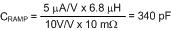
The next lowest standard value 270 pF was selected for CRAMP. An NPO capacitor with 5% or better tolerance is recommended. Note that selecting a capacitor value lower than the calculated value increases the slope compensation. Furthermore, selecting a ramp capacitor substantially lower or higher than the calculated value also results in incorrect PWM operation.
For VOUT > 5 V, internal slope compensation provided by the LM25088 may not be adequate for certain operating conditions especially at low input voltages. A pullup resistor may be added from the VCC to RAMP pin to increase the slope compensation. Optimal slope compensation current can be calculated from:
and RRAMP is given by
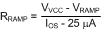
 Figure 8-3 Additional Slope Compensation for
VOUT > 5 V
Figure 8-3 Additional Slope Compensation for
VOUT > 5 V