ZHCSQP4K December 2008 – June 2022 LM25088 , LM25088-Q1
PRODUCTION DATA
- 1 特性
- 2 应用
- 3 说明
- 4 Revision History
- 5 Pin Configuration and Functions
- 6 Specifications
-
7 Detailed Description
- 7.1 Overview
- 7.2 Functional Block Diagram
- 7.3
Feature Description
- 7.3.1 High Voltage Low-Dropout Regulator
- 7.3.2 Line Undervoltage Detector
- 7.3.3 Oscillator and Sync Capability
- 7.3.4 Error Amplifier and PWM Comparator
- 7.3.5 Ramp Generator
- 7.3.6 Dropout Voltage Reduction
- 7.3.7 Frequency Dithering (LM25088-1 Only)
- 7.3.8 Cycle-by-Cycle Current Limit
- 7.3.9 Overload Protection Timer (LM25088-2 Only)
- 7.3.10 Soft Start
- 7.3.11 HG Output
- 7.3.12 Thermal Protection
- 7.4 Device Functional Modes
-
8 Application and Implementation
- 8.1 Application Information
- 8.2
Typical Application
- 8.2.1 Design Requirements
- 8.2.2
Detailed Design Procedure
- 8.2.2.1 Timing Resistor
- 8.2.2.2 Output Inductor
- 8.2.2.3 Current Sense Resistor
- 8.2.2.4 Ramp Capacitor
- 8.2.2.5 Output Capacitors
- 8.2.2.6 Input Capacitors
- 8.2.2.7 VCC Capacitor
- 8.2.2.8 Bootstrap Capacitor
- 8.2.2.9 Soft-Start Capacitor
- 8.2.2.10 Output Voltage Divider
- 8.2.2.11 UVLO Divider
- 8.2.2.12 Restart Capacitor (LM5008-2 Only)
- 8.2.2.13 MOSFET Selection
- 8.2.2.14 Diode Selection
- 8.2.2.15 Snubber Components Selection
- 8.2.2.16 Error Amplifier Compensation
- 8.2.3 Application Curves
- 9 Power Supply Recommendations
- 10Layout
- 11Device and Documentation Support
- 12Mechanical, Packaging, and Orderable Information
7.3.5 Ramp Generator
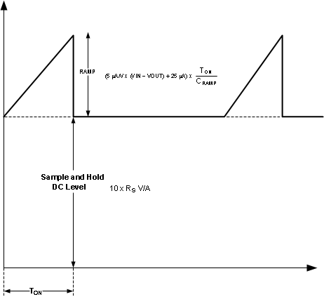
The ramp signal used for the pulse width modulator in current mode control is typically derived directly from the buck switch current. This signal corresponds to the positive slope portion of the buck inductor current. Using this signal for the PWM ramp simplifies the control loop transfer function to a single pole response and provides inherent input voltage feedforward compensation. The disadvantage of using the buck switch current signal for PWM control is the large leading edge spike due to circuit parasitics which must be filtered or blanked. Also, the current measurement can introduce significant propagation delays. The filtering time, blanking time, and propagation delay limit the minimum achievable pulse width. In applications where the input voltage can be relatively large in comparison to the output voltage, controlling small pulse widths and duty cycles is necessary for regulation. The LM25088 utilizes a unique ramp generator, which does not actually measure the buck switch current but rather reconstructs or emulates the signal. Emulating the inductor current provides a ramp signal that is free of leading edge spikes and measurement or filtering delays. The current reconstruction is comprised of two elements: a sample and hold DC level and an emulated current ramp.
 Figure 7-3 Composition of Current Sense Signal
The sample and hold DC level illustrated in Figure 7-3 is derived from a measurement of the re-circulating (or free-wheeling) diode current. The diode current flows through the current sense resistor connected between the CS and CSG pins. The voltage across the sense resistor is sampled and held just prior to the onset of the next conduction interval of the buck switch. The diode current sensing and sample and hold provide the DC level for the reconstructed current signal. The positive slope inductor current ramp is emulated by an external capacitor connected from the RAMP pin to GND and an internal voltage controlled current source. The ramp current source that emulates the inductor current is a function of the VIN and VOUT voltages per the following equation:
Proper selection of the RAMP capacitor depends upon the selected value of the output inductor and the current sense resistor (RS). For proper current emulation, the DC sample and hold value and the ramp amplitude must have the same dependence on the load current. That is:

where
- gm is the ramp current generator transconductance (5 µA/V).
- A is the gain of the current sense amplifier (10 V/V).
The RAMP capacitor must connected directly to the RAMP and GND pins of the IC.
For duty cycles greater than 50%, peak current mode control circuits are subject to subharmonic oscillation. Subharmonic oscillation is normally characterized by alternating wide and narrow pulses at the SW pin. Adding a fixed slope voltage ramp (slope compensation) to the current sense signal prevents this oscillation. The 25-µA offset current supplied by the emulated current source provides a fixed slope to the ramp signal. In some high output voltage, high duty cycle applications, additional slope compensation can be required. In these applications, a pullup resistor can be added between the RAMP and VCC pins to increase the ramp slope compensation. A formula to configure pullup resistor is shown in Section 8.