ZHCSQP4K December 2008 – June 2022 LM25088 , LM25088-Q1
PRODUCTION DATA
- 1 特性
- 2 应用
- 3 说明
- 4 Revision History
- 5 Pin Configuration and Functions
- 6 Specifications
-
7 Detailed Description
- 7.1 Overview
- 7.2 Functional Block Diagram
- 7.3
Feature Description
- 7.3.1 High Voltage Low-Dropout Regulator
- 7.3.2 Line Undervoltage Detector
- 7.3.3 Oscillator and Sync Capability
- 7.3.4 Error Amplifier and PWM Comparator
- 7.3.5 Ramp Generator
- 7.3.6 Dropout Voltage Reduction
- 7.3.7 Frequency Dithering (LM25088-1 Only)
- 7.3.8 Cycle-by-Cycle Current Limit
- 7.3.9 Overload Protection Timer (LM25088-2 Only)
- 7.3.10 Soft Start
- 7.3.11 HG Output
- 7.3.12 Thermal Protection
- 7.4 Device Functional Modes
-
8 Application and Implementation
- 8.1 Application Information
- 8.2
Typical Application
- 8.2.1 Design Requirements
- 8.2.2
Detailed Design Procedure
- 8.2.2.1 Timing Resistor
- 8.2.2.2 Output Inductor
- 8.2.2.3 Current Sense Resistor
- 8.2.2.4 Ramp Capacitor
- 8.2.2.5 Output Capacitors
- 8.2.2.6 Input Capacitors
- 8.2.2.7 VCC Capacitor
- 8.2.2.8 Bootstrap Capacitor
- 8.2.2.9 Soft-Start Capacitor
- 8.2.2.10 Output Voltage Divider
- 8.2.2.11 UVLO Divider
- 8.2.2.12 Restart Capacitor (LM5008-2 Only)
- 8.2.2.13 MOSFET Selection
- 8.2.2.14 Diode Selection
- 8.2.2.15 Snubber Components Selection
- 8.2.2.16 Error Amplifier Compensation
- 8.2.3 Application Curves
- 9 Power Supply Recommendations
- 10Layout
- 11Device and Documentation Support
- 12Mechanical, Packaging, and Orderable Information
7.3.7 Frequency Dithering (LM25088-1 Only)
Electro-magnetic interference (EMI) emissions are fundamentally associated with switch-mode power supplies due to sharp voltage transitions, diode reverse recovery currents, and the ringing of parasitic L-C circuits. These emissions conduct back to the power source or radiate into the environment and potentially interfere with nearby electronic systems. System designers typically use a combination of shielding, filtering, and layout techniques to reduce the EMI emissions sufficiently to satisfy EMI emission standards established by regulatory bodies. In a typical fixed frequency switching converter, narrowband emissions typically peak at the switching frequency with the successive harmonics having less energy. Dithering the oscillator frequency spreads the EMI energy over a range of frequencies, thus reducing the peak levels. Dithering can also reduce the system cost by reducing the size and quantity of EMI filtering components.
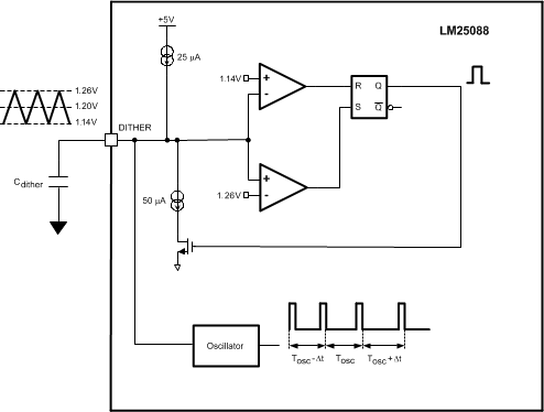
The LM25088-1 provides an optional frequency dithering function, which is enabled by connecting a capacitor from the dither pin (DITH) to GND. Connecting the DITH pin directly to GND disables frequency dithering causing the oscillator to operate at the frequency established by the RT resistor. As shown in Figure 7-5, the Cdither capacitor is used to generate a triangular wave centered at 1.2 V. This triangular waveform is used to manipulate the oscillator circuit such that the oscillator frequency modulates from –5% to +5% of the nominal operating frequency set by the RT resistor. The Cdither capacitor value sets the rate of the low frequency modulation. For example, a lower value Cdither capacitor modulates the oscillator frequency from –5% to +5% at a faster rate than a higher value capacitor. For the dither circuit to work effectively, the modulation rate must be much less than the oscillator frequency (fSW). Select Cdither such that:

 Figure 7-5 Frequency Dithering Scheme
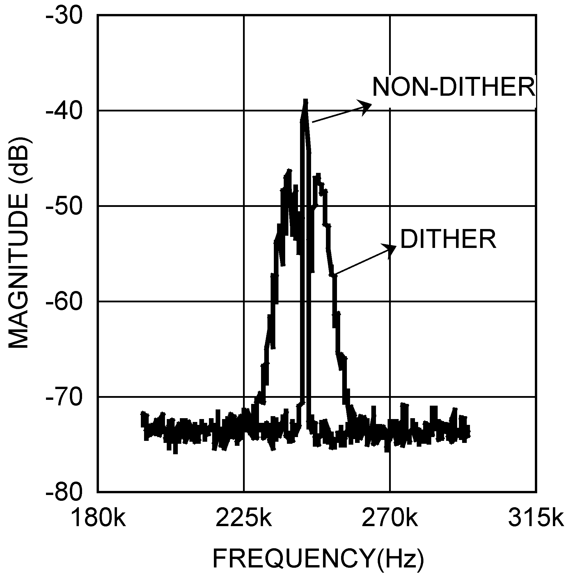
 Figure 7-6 Conducted Emissions Measured at the Input of a
LM25088-Based Buck Converter
Figure 7-6 Conducted Emissions Measured at the Input of a
LM25088-Based Buck ConverterFigure 7-6 shows the conducted emissions on the LM25088 evaluation board input power line. It can be seen from the above picture that, the peak emissions with non-dithering operation are centered narrowly at the operating frequency of the converter. With dithering operation, the conducted emissions are spread around the operating frequency and the maximum amplitude is reduced by approximately 10 dB. Figure 7-6 was captured using a Chroma DC power supply model number 62006P and an Agilent network analyzer model number 4395A.