ZHCSQP4K December 2008 – June 2022 LM25088 , LM25088-Q1
PRODUCTION DATA
- 1 特性
- 2 应用
- 3 说明
- 4 Revision History
- 5 Pin Configuration and Functions
- 6 Specifications
-
7 Detailed Description
- 7.1 Overview
- 7.2 Functional Block Diagram
- 7.3
Feature Description
- 7.3.1 High Voltage Low-Dropout Regulator
- 7.3.2 Line Undervoltage Detector
- 7.3.3 Oscillator and Sync Capability
- 7.3.4 Error Amplifier and PWM Comparator
- 7.3.5 Ramp Generator
- 7.3.6 Dropout Voltage Reduction
- 7.3.7 Frequency Dithering (LM25088-1 Only)
- 7.3.8 Cycle-by-Cycle Current Limit
- 7.3.9 Overload Protection Timer (LM25088-2 Only)
- 7.3.10 Soft Start
- 7.3.11 HG Output
- 7.3.12 Thermal Protection
- 7.4 Device Functional Modes
-
8 Application and Implementation
- 8.1 Application Information
- 8.2
Typical Application
- 8.2.1 Design Requirements
- 8.2.2
Detailed Design Procedure
- 8.2.2.1 Timing Resistor
- 8.2.2.2 Output Inductor
- 8.2.2.3 Current Sense Resistor
- 8.2.2.4 Ramp Capacitor
- 8.2.2.5 Output Capacitors
- 8.2.2.6 Input Capacitors
- 8.2.2.7 VCC Capacitor
- 8.2.2.8 Bootstrap Capacitor
- 8.2.2.9 Soft-Start Capacitor
- 8.2.2.10 Output Voltage Divider
- 8.2.2.11 UVLO Divider
- 8.2.2.12 Restart Capacitor (LM5008-2 Only)
- 8.2.2.13 MOSFET Selection
- 8.2.2.14 Diode Selection
- 8.2.2.15 Snubber Components Selection
- 8.2.2.16 Error Amplifier Compensation
- 8.2.3 Application Curves
- 9 Power Supply Recommendations
- 10Layout
- 11Device and Documentation Support
- 12Mechanical, Packaging, and Orderable Information
8.2.2.5 Output Capacitors
The output capacitors smooth the inductor current ripple and provide a source of charge for load transient conditions. The output capacitor selection is primarily dictated by the following specifications:
- Steady-state output peak-peak ripple (ΔVPK-PK)
- Output voltage deviation during transient condition (ΔVTransient)
For the 5-V output design example, ΔVPK-PK = 50 mV (1% of VOUT) and ΔTTransient = 100 mV (2% of VOUT) were chosen. The magnitude of output ripple primarily depends on ESR of the capacitors while load transient voltage deviation depends both on the output capacitance and ESR.
When a full load is suddenly removed from the output, the output capacitor must be large enough to prevent the inductor energy to raise the output voltage above the specified maximum voltage. In other words, the output capacitor must be large enough to absorb the maximum stored energy of the inductor. The stored energy equations of both the inductor and the output capacitor can be calculated:
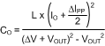
Evaluating, the above equation with a ΔVout of 100 mV results in an output capacitance of 475 µF. As stated earlier, the maximum peak to peak ripple primarily depends on the ESR of the output capacitor and the inductor ripple current. To satisfy the ΔVPK-PK of 50 mV with 40% inductor current ripple, the ESR must be less than 15 mΩ. In this design example, a 470-µF aluminum capacitor with an ESR of 10 mΩ is paralleled with two 47-µF ceramic capacitors to further reduce the ESR.