SWRS283A June 2022 – November 2022 IWR6243
PRODUCTION DATA
- 1 Features
- 2 Applications
- 3 Description
- 4 Functional Block Diagram
- 5 Revision History
- 6 Device Comparison
- 7 Terminal Configuration and Functions
-
8 Specifications
- 8.1 Absolute Maximum Ratings
- 8.2 ESD Ratings
- 8.3 Power-On Hours (POH)
- 8.4 Recommended Operating Conditions
- 8.5 Power Supply Specifications
- 8.6 Power Consumption Summary
- 8.7 RF Specification
- 8.8 Thermal Resistance Characteristics for FCBGA Package [ABL0161]
- 8.9
Timing and Switching Characteristics
- 8.9.1 Power Supply Sequencing and Reset Timing
- 8.9.2 Synchronized Frame Triggering
- 8.9.3 Input Clocks and Oscillators
- 8.9.4 Multibuffered / Standard Serial Peripheral Interface (MibSPI)
- 8.9.5 Inter-Integrated Circuit Interface (I2C)
- 8.9.6 LVDS Interface Configuration
- 8.9.7 General-Purpose Input/Output
- 8.9.8 Camera Serial Interface (CSI2)
- 9 Detailed Description
- 10Monitoring and Diagnostic Mechanisms
- 11Applications, Implementation, and Layout
- 12Device and Documentation Support
- 13Mechanical, Packaging, and Orderable Information
9.4.2 ADC Channels (Service) for User Application
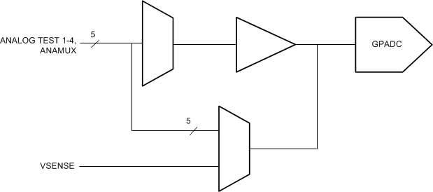
The device includes provision for an ADC service for user application, where the GPADC engine present inside the device can be used to measure up to six external voltages. The ADC1, ADC2, ADC3, ADC4, ADC5, and ADC6 pins are used for this purpose.
- ADC itself is controlled by TI firmware running inside the BIST subsystem and access to it for customer’s external voltage monitoring purpose is via ‘monitoring API’ calls routed to the BIST subsystem. This API could be linked with the user application running on the MSS R4F.
- BIST subsystem firmware will internally schedule these measurements along with other RF and Analog monitoring operations. The API allows configuring the settling time (number of ADC samples to skip) and number of consecutive samples to take. At the end of a frame, the minimum, maximum and average of the readings will be reported for each of the monitored voltages.
GPADC Specifications:
- 625 Ksps SAR ADC
- 0 to 1.8V input range
- 10-bit resolution
- For 5 out of the 6 inputs, an optional internal buffer is available. Without the buffer, the ADC has a switched capacitor input load modeled with 5pF of sampling capacitance and 12pF parasitic capacitance (GPADC channel 6, the internal buffer is not available).

A. GPADC structures are used for measuring the
output of internal temperature sensors. The accuracy of these measurements is
±7°C.
Figure 9-6 ADC Path