ZHCSI69B june 2018 – september 2020 DS90C189-Q1
PRODUCTION DATA
- 1
- 1 特性
- 2 应用
- 3 说明
- 4 Typical Application Diagrams
- 5 Revision History
- 6 Pin Configuration and Functions
- 7 Specifications
- 8 Detailed Description
- 9 Application and Implementation
- 10Power Supply Recommendations
- 11Layout
- 12Device and Documentation Support
- 13Mechanical, Packaging, and Orderable Information
7.8 AC Timing Diagrams
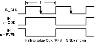
A. The worst case test pattern produces a maximum toggling of digital circuits, LVDS I/O and LVCMOS/ I/O.
B. Figure 7-2 shows a falling edge data strobe (IN_CLK).
Figure 7-1 Checker Board Test Pattern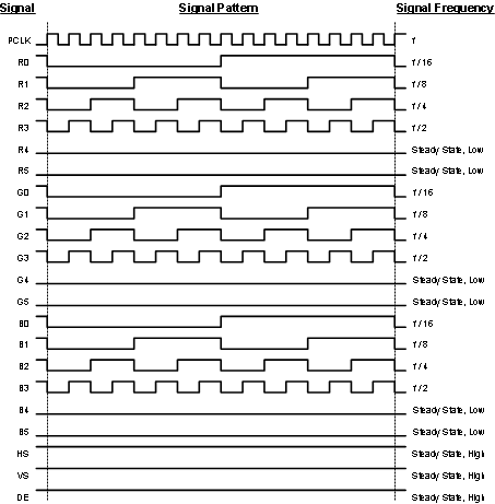
A. The worst case test pattern produces a maximum toggling of digital circuits, LVDS I/O and LVCMOS/ I/O.
B. Recommended pin to signal mapping for 18 bits per pixel, customer may choose to define differently. The 16 grayscale test pattern tests device power consumption for a “typical” LCD display pattern. The test pattern approximates signal switching needed to produce groups of 16 vertical stripes across the display.
C. Figure 7-2 shows a falling edge data strobe (IN_CLK).
Figure 7-2 “16 Gray Scale” Test Pattern (Falling Edge Clock shown) Figure 7-3 DS90C189-Q1 (Transmitter) LVDS Output Load
 Figure 7-4 LVDS Output Transition Times
 Figure 7-5 LVCMOS Input Transition Times
 Figure 7-6 LVCMOS Input Setup/Hold and Clock High/Low Times (Falling Edge Strobe)
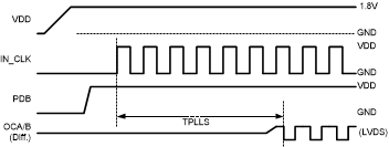 Figure 7-7 Start Up / Phase Lock Loop Set Time
 Figure 7-8 Sleep Mode / Power Down Delay
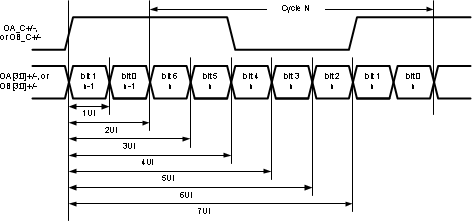 Figure 7-9 LVDS Serial Bit Positions
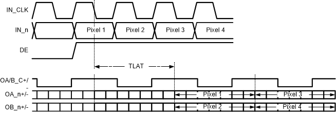 Figure 7-10 Single In, Dual Out Mode Timing and Latency
 Figure 7-11 Single In, Single Out Mode Timing and Latency