ZHCSI52G August   2016  – March 2019 DRA780 , DRA781 , DRA782 , DRA783 , DRA785 , DRA786 , DRA787 , DRA788

PRODUCTION DATA.  

  1. 1器件概述
    1. 1.1 特性
    2. 1.2 应用
    3. 1.3 说明
    4. 1.4 功能框图
  2. 2修订历史记录
  3. 3Device Comparison
    1. 3.1 Related Products
  4. 4Terminal Configuration and Functions
    1. 4.1 Pin Diagram
    2. 4.2 Pin Attributes
    3. 4.3 Signal Descriptions
      1. 4.3.1  VIP
      2. 4.3.2  DSS
      3. 4.3.3  SD_DAC
      4. 4.3.4  ADC
      5. 4.3.5  Camera Control
      6. 4.3.6  CPI
      7. 4.3.7  CSI2
      8. 4.3.8  EMIF
      9. 4.3.9  GPMC
      10. 4.3.10 Timers
      11. 4.3.11 I2C
      12. 4.3.12 UART
      13. 4.3.13 McSPI
      14. 4.3.14 QSPI
      15. 4.3.15 McASP
      16. 4.3.16 DCAN and MCAN
      17. 4.3.17 GMAC_SW
      18. 4.3.18 SDIO Controller
      19. 4.3.19 GPIO
      20. 4.3.20 ePWM
      21. 4.3.21 ATL
      22. 4.3.22 Test Interfaces
      23. 4.3.23 System and Miscellaneous
        1. 4.3.23.1 Sysboot
        2. 4.3.23.2 Power, Reset and Clock Management (PRCM)
        3. 4.3.23.3 Enhanced Direct Memory Access (EDMA)
        4. 4.3.23.4 Interrupt Controllers (INTC)
      24. 4.3.24 Power Supplies
    4. 4.4 Pin Multiplexing
    5. 4.5 Connections for Unused Pins
  5. 5Specifications
    1. 5.1 Absolute Maximum Ratings
    2. 5.2 ESD Ratings
    3. 5.3 Power on Hour (POH) Limits
    4. 5.4 Recommended Operating Conditions
    5. 5.5 Operating Performance Points
      1. 5.5.1 AVS Requirements
      2. 5.5.2 Voltage And Core Clock Specifications
      3. 5.5.3 Maximum Supported Frequency
    6. 5.6 Power Consumption Summary
    7. 5.7 Electrical Characteristics
      1. Table 5-6  LVCMOS DDR DC Electrical Characteristics
      2. Table 5-7  Dual Voltage LVCMOS I2C DC Electrical Characteristics
      3. Table 5-8  IQ1833 Buffers DC Electrical Characteristics
      4. Table 5-9  IHHV1833 Buffers DC Electrical Characteristics
      5. Table 5-10 LVCMOS Analog OSC Buffers DC Electrical Characteristics
      6. Table 5-11 Dual Voltage LVCMOS DC Electrical Characteristics
      7. Table 5-12 Analog-to-Digital ADC Subsystem Electrical Specifications
    8. 5.8 Thermal Characteristics
      1. 5.8.1 Package Thermal Characteristics
    9. 5.9 Timing Requirements and Switching Characteristics
      1. 5.9.1 Timing Parameters and Information
        1. 5.9.1.1 Parameter Information
          1. 5.9.1.1.1 1.8 V and 3.3 V Signal Transition Levels
          2. 5.9.1.1.2 1.8 V and 3.3 V Signal Transition Rates
          3. 5.9.1.1.3 Timing Parameters and Board Routing Analysis
      2. 5.9.2 Interface Clock Specifications
        1. 5.9.2.1 Interface Clock Terminology
        2. 5.9.2.2 Interface Clock Frequency
      3. 5.9.3 Power Supply Sequences
      4. 5.9.4 Clock Specifications
        1. 5.9.4.1 Input Clocks / Oscillators
          1. 5.9.4.1.1 OSC0 External Crystal
          2. 5.9.4.1.2 OSC0 Input Clock
          3. 5.9.4.1.3 Auxiliary Oscillator OSC1 Input Clock
            1. 5.9.4.1.3.1 OSC1 External Crystal
            2. 5.9.4.1.3.2 OSC1 Input Clock
          4. 5.9.4.1.4 RC On-die Oscillator Clock
        2. 5.9.4.2 Output Clocks
        3. 5.9.4.3 DPLLs, DLLs
          1. 5.9.4.3.1 DPLL Characteristics
          2. 5.9.4.3.2 DLL Characteristics
            1. 5.9.4.3.2.1 DPLL and DLL Noise Isolation
      5. 5.9.5 Recommended Clock and Control Signal Transition Behavior
      6. 5.9.6 Peripherals
        1. 5.9.6.1  Timing Test Conditions
        2. 5.9.6.2  VIP
        3. 5.9.6.3  DSS
        4. 5.9.6.4  EMIF
        5. 5.9.6.5  GPMC
          1. 5.9.6.5.1 GPMC/NOR Flash Interface Synchronous Timing
          2. 5.9.6.5.2 GPMC/NOR Flash Interface Asynchronous Timing
          3. 5.9.6.5.3 GPMC/NAND Flash Interface Asynchronous Timing
        6. 5.9.6.6  GP Timers
          1. 5.9.6.6.1 GP Timer Features
        7. 5.9.6.7  I2C
          1. Table 5-39 Timing Requirements for I2C Input Timings
          2. Table 5-40 Switching Characteristics Over Recommended Operating Conditions for I2C Output Timings
        8. 5.9.6.8  UART
          1. Table 5-41 Timing Requirements for UART
          2. Table 5-42 Switching Characteristics Over Recommended Operating Conditions for UART
        9. 5.9.6.9  McSPI
        10. 5.9.6.10 QSPI
        11. 5.9.6.11 McASP
          1. Table 5-50 Timing Requirements for McASP1
          2. Table 5-51 Timing Requirements for McASP2
          3. Table 5-52 Timing Requirements for McASP3
          4. Table 5-53 Switching Characteristics Over Recommended Operating Conditions for McASP1
          5. Table 5-54 Switching Characteristics Over Recommended Operating Conditions for McASP2
          6. Table 5-55 Switching Characteristics Over Recommended Operating Conditions for McASP3
        12. 5.9.6.12 DCAN and MCAN
          1. 5.9.6.12.1 DCAN
          2. 5.9.6.12.2 MCAN
          3. Table 5-58 Timing Requirements for CAN Receive
          4. Table 5-59 Switching Characteristics Over Recommended Operating Conditions for CAN Transmit
        13. 5.9.6.13 GMAC_SW
          1. 5.9.6.13.1 GMAC MDIO Interface Timings
          2. 5.9.6.13.2 GMAC RGMII Timings
            1. Table 5-63 Timing Requirements for rgmiin_rxc - RGMIIn Operation
            2. Table 5-64 Timing Requirements for GMAC RGMIIn Input Receive for 10/100/1000 Mbps
            3. Table 5-65 Switching Characteristics Over Recommended Operating Conditions for rgmiin_txctl - RGMIIn Operation for 10/100/1000 Mbit/s
            4. Table 5-66 Switching Characteristics for GMAC RGMIIn Output Transmit for 10/100/1000 Mbps
        14. 5.9.6.14 SDIO Controller
          1. 5.9.6.14.1 MMC, SD Default Speed
          2. 5.9.6.14.2 MMC, SD High Speed
          3. 5.9.6.14.3 MMC, SD and SDIO SDR12 Mode
          4. 5.9.6.14.4 MMC, SD SDR25 Mode
        15. 5.9.6.15 GPIO
        16. 5.9.6.16 ATL
          1. 5.9.6.16.1 ATL Electrical Data/Timing
            1. Table 5-77 Switching Characteristics Over Recommended Operating Conditions for ATL_CLKOUTx
      7. 5.9.7 Emulation and Debug Subsystem
        1. 5.9.7.1 JTAG Electrical Data/Timing
          1. Table 5-78 Timing Requirements for IEEE 1149.1 JTAG
          2. Table 5-79 Switching Characteristics Over Recommended Operating Conditions for IEEE 1149.1 JTAG
          3. Table 5-80 Timing Requirements for IEEE 1149.1 JTAG With RTCK
          4. Table 5-81 Switching Characteristics Over Recommended Operating Conditions for IEEE 1149.1 JTAG With RTCK
        2. 5.9.7.2 Trace Port Interface Unit (TPIU)
          1. 5.9.7.2.1 TPIU PLL DDR Mode
  6. 6Detailed Description
    1. 6.1  Description
    2. 6.2  Functional Block Diagram
    3. 6.3  DSP Subsystem
    4. 6.4  IPU
    5. 6.5  EVE
    6. 6.6  Memory Subsystem
      1. 6.6.1 EMIF
      2. 6.6.2 GPMC
      3. 6.6.3 ELM
      4. 6.6.4 OCMC
    7. 6.7  Interprocessor Communication
      1. 6.7.1 Mailbox
      2. 6.7.2 Spinlock
    8. 6.8  Interrupt Controller
    9. 6.9  EDMA
    10. 6.10 Peripherals
      1. 6.10.1  VIP
      2. 6.10.2  DSS
      3. 6.10.3  ATL
      4. 6.10.4  ADC
      5. 6.10.5  Timers
        1. 6.10.5.1 General-Purpose Timers
        2. 6.10.5.2 32-kHz Synchronized Timer (COUNTER_32K)
      6. 6.10.6  I2C
      7. 6.10.7  UART
        1. 6.10.7.1 UART Features
      8. 6.10.8  McSPI
      9. 6.10.9  QSPI
      10. 6.10.10 McASP
      11. 6.10.11 DCAN
      12. 6.10.12 MCAN
      13. 6.10.13 GMAC_SW
      14. 6.10.14 SDIO
      15. 6.10.15 GPIO
      16. 6.10.16 ePWM
      17. 6.10.17 eCAP
      18. 6.10.18 eQEP
    11. 6.11 On-Chip Debug
  7. 7Applications, Implementation, and Layout
    1. 7.1 Introduction
      1. 7.1.1 Initial Requirements and Guidelines
    2. 7.2 Power Optimizations
      1. 7.2.1 Step 1: PCB Stack-up
      2. 7.2.2 Step 2: Physical Placement
      3. 7.2.3 Step 3: Static Analysis
        1. 7.2.3.1 PDN Resistance and IR Drop
      4. 7.2.4 Step 4: Frequency Analysis
      5. 7.2.5 System ESD Generic Guidelines
        1. 7.2.5.1 System ESD Generic PCB Guideline
        2. 7.2.5.2 Miscellaneous EMC Guidelines to Mitigate ESD Immunity
        3. 7.2.5.3 ESD Protection System Design Consideration
      6. 7.2.6 EMI / EMC Issues Prevention
        1. 7.2.6.1 Signal Bandwidth
        2. 7.2.6.2 Signal Routing
          1. 7.2.6.2.1 Signal Routing—Sensitive Signals and Shielding
          2. 7.2.6.2.2 Signal Routing—Outer Layer Routing
        3. 7.2.6.3 Ground Guidelines
          1. 7.2.6.3.1 PCB Outer Layers
          2. 7.2.6.3.2 Metallic Frames
          3. 7.2.6.3.3 Connectors
          4. 7.2.6.3.4 Guard Ring on PCB Edges
          5. 7.2.6.3.5 Analog and Digital Ground
    3. 7.3 Core Power Domains
      1. 7.3.1 General Constraints and Theory
      2. 7.3.2 Voltage Decoupling
      3. 7.3.3 Static PDN Analysis
      4. 7.3.4 Dynamic PDN Analysis
      5. 7.3.5 Power Supply Mapping
      6. 7.3.6 DPLL Voltage Requirement
      7. 7.3.7 Loss of Input Power Event
      8. 7.3.8 Example PCB Design
        1. 7.3.8.1 Example Stack-up
        2. 7.3.8.2 vdd_dspeve Example Analysis
    4. 7.4 Single-Ended Interfaces
      1. 7.4.1 General Routing Guidelines
      2. 7.4.2 QSPI Board Design and Layout Guidelines
        1. 7.4.2.1 If QSPI is operated in Mode 0 (POL=0, PHA=0):
        2. 7.4.2.2 If QSPI is operated in Mode 3 (POL=1, PHA=1):
    5. 7.5 Differential Interfaces
      1. 7.5.1 General Routing Guidelines
    6. 7.6 Clock Routing Guidelines
      1. 7.6.1 Oscillator Ground Connection
    7. 7.7 DDR2 Board Design and Layout Guidelines
      1. 7.7.1 DDR2 General Board Layout Guidelines
      2. 7.7.2 DDR2 Board Design and Layout Guidelines
        1. 7.7.2.1 Board Designs
        2. 7.7.2.2 DDR2 Interface
          1. 7.7.2.2.1  DDR2 Interface Schematic
          2. 7.7.2.2.2  Compatible JEDEC DDR2 Devices
          3. 7.7.2.2.3  PCB Stackup
          4. 7.7.2.2.4  Placement
          5. 7.7.2.2.5  DDR2 Keepout Region
          6. 7.7.2.2.6  Bulk Bypass Capacitors
          7. 7.7.2.2.7  High-Speed Bypass Capacitors
          8. 7.7.2.2.8  Net Classes
          9. 7.7.2.2.9  DDR2 Signal Termination
          10. 7.7.2.2.10 VREF Routing
        3. 7.7.2.3 DDR2 CK and ADDR_CTRL Routing
    8. 7.8 DDR3 Board Design and Layout Guidelines
      1. 7.8.1 DDR3 General Board Layout Guidelines
      2. 7.8.2 DDR3 Board Design and Layout Guidelines
        1. 7.8.2.1  Board Designs
        2. 7.8.2.2  DDR3 Device Combinations
        3. 7.8.2.3  DDR3 Interface Schematic
          1. 7.8.2.3.1 32-Bit DDR3 Interface
          2. 7.8.2.3.2 16-Bit DDR3 Interface
        4. 7.8.2.4  Compatible JEDEC DDR3 Devices
        5. 7.8.2.5  PCB Stackup
        6. 7.8.2.6  Placement
        7. 7.8.2.7  DDR3 Keepout Region
        8. 7.8.2.8  Bulk Bypass Capacitors
        9. 7.8.2.9  High-Speed Bypass Capacitors
          1. 7.8.2.9.1 Return Current Bypass Capacitors
        10. 7.8.2.10 Net Classes
        11. 7.8.2.11 DDR3 Signal Termination
        12. 7.8.2.12 VTT
        13. 7.8.2.13 CK and ADDR_CTRL Topologies and Routing Definition
          1. 7.8.2.13.1 Three DDR3 Devices
            1. 7.8.2.13.1.1 CK and ADDR_CTRL Topologies, Three DDR3 Devices
            2. 7.8.2.13.1.2 CK and ADDR_CTRL Routing, Three DDR3 Devices
          2. 7.8.2.13.2 Two DDR3 Devices
            1. 7.8.2.13.2.1 CK and ADDR_CTRL Topologies, Two DDR3 Devices
            2. 7.8.2.13.2.2 CK and ADDR_CTRL Routing, Two DDR3 Devices
          3. 7.8.2.13.3 One DDR3 Device
            1. 7.8.2.13.3.1 CK and ADDR_CTRL Topologies, One DDR3 Device
            2. 7.8.2.13.3.2 CK and ADDR/CTRL Routing, One DDR3 Device
        14. 7.8.2.14 Data Topologies and Routing Definition
          1. 7.8.2.14.1 DQS and DQ/DM Topologies, Any Number of Allowed DDR3 Devices
          2. 7.8.2.14.2 DQS and DQ/DM Routing, Any Number of Allowed DDR3 Devices
        15. 7.8.2.15 Routing Specification
          1. 7.8.2.15.1 CK and ADDR_CTRL Routing Specification
          2. 7.8.2.15.2 DQS and DQ Routing Specification
    9. 7.9 CVIDEO/SD-DAC Guidelines and Electrical Data/Timing
  8. 8Device and Documentation Support
    1. 8.1 Device Nomenclature
      1. 8.1.1 Standard Package Symbolization
      2. 8.1.2 Device Naming Convention
    2. 8.2 Tools and Software
    3. 8.3 Documentation Support
    4. 8.4 Related Links
    5. 8.5 Community Resources
    6. 8.6 商标
    7. 8.7 静电放电警告
    8. 8.8 Export Control Notice
    9. 8.9 Glossary
  9. 9Mechanical, Packaging, and Orderable Information
    1. 9.1 Packaging Information

封装选项

请参考 PDF 数据表获取器件具体的封装图。

机械数据 (封装 | 引脚)
  • ABF|367
散热焊盘机械数据 (封装 | 引脚)
订购信息

DDR2 CK and ADDR_CTRL Routing

Figure 7-29 shows the topology of the routing for the CK and ADDR_CTRL net classes. The route is a point to point connection with required skew matching.
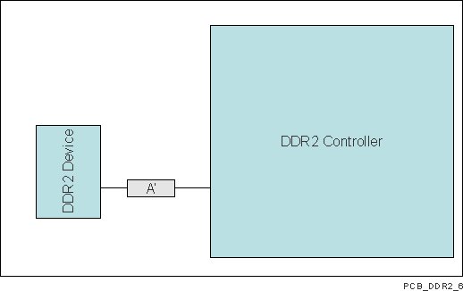
DRA780 DRA781 DRA782 DRA783 DRA784 DRA785 DRA786 DRA787 DRA788 SPRS949_PCB_DDR2_6.gifFigure 7-29 CK and ADDR_CTRL Routing and Topology

Table 7-20 CK and ADDR_CTRL Routing Specification

NO. PARAMETER MIN MAX UNIT
RSC21 Center-to-center ddrx_ck - ddrx_nck spacing 2w
RSC22 ddrx_ck / ddrx_nck skew 5 ps
RSC25 Center-to-center CK to other DDR2 trace spacing(2) 4w
RSC26 CK/ADDR_CTRL trace length(3) 680 ps
RSC27 ADDR_CTRL-to-CK skew mismatch 25 ps
RSC28 ADDR_CTRL-to-ADDR_CTRL skew mismatch 25 ps
RSC29 Center-to-center ADDR_CTRL to other DDR2 trace spacing(2) 4w
RSC210 Center-to-center ADDR_CTRL to other ADDR_CTRL trace spacing(2) 3w
  1. Series terminator, if used, should be located closest to the Device.
  2. Center-to-center spacing is allowed to fall to minimum 2w for up to 500 mils of routed length to accommodate BGA escape and routing congestion.
  3. This is the longest routing length of the CK and ADDR_CTRL net classes.

Figure 7-30 shows the topology and routing for the DQS and DQ net classes; the routes are point to point. Skew matching across bytes is not needed nor recommended. The termination resistor should be placed near the processor.
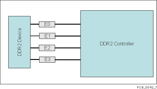
DRA780 DRA781 DRA782 DRA783 DRA784 DRA785 DRA786 DRA787 DRA788 SPRS949_PCB_DDR2_7.gifFigure 7-30 DQS and DQ Routing and Topology

Table 7-21 DQS and DQ Routing Specification

NO. PARAMETER MIN MAX UNIT
RSDQ21 Center-to-center DQS-DQSn spacing in E0|E1|E2|E3 2w
RSDQ22 DQS-DQSn skew in E0|E1|E2|E3 5 ps
RSDQ23 Center-to-center DQS to other DDR2 trace spacing(1) 4w
RSDQ24 DQS/DQ trace length (2)(3)(4) 325 ps
RSDQ25 DQ-to-DQS skew mismatch(2)(3)(4) 10 ps
RSDQ26 DQ-to-DQ skew mismatch(2)(3)(4) 10 ps
RSDQ27 DQ-to-DQ/DQS via count mismatch(2)(3)(4) 1 Vias
RSDQ28 Center-to-center DQ to other DDR2 trace spacing(1)(5) 4w
RSDQ29 Center-to-center DQ to other DQ trace spacing(1)(6)(7) 3w
RSDQ210 DQ/DQS E skew mismatch(2)(3)(4) 25 ps
  1. Center-to-center spacing is allowed to fall to minimum 2w for up to 500 mils of routed length to accommodate BGA escape and routing congestion.
  2. A 16-bit DDR memory system has two sets of data net classes; one for data byte 0, and one for data byte 1, each with an associated DQS (2 DQSs) per DDR EMIF used.
  3. A 32-bit DDR memory system has four sets of data net classes; one each for data bytes 0 through 3, and each associated with a DQS (4 DQSs) per DDR EMIF used.
  4. There is no need, and it is not recommended, to skew match across data bytes; that is, from DQS0 and data byte 0 to DQS1 and data byte1.
  5. DQs from other DQS domains are considered other DDR2 trace.
  6. DQs from other data bytes are considered other DDR2 trace.
  7. This is the longest routing distance of each of the DQS and DQ net classes.