ZHCSHA4B July   2007  – January 2018 DAC8881

PRODUCTION DATA.  

  1. 特性
  2. 应用
  3. 说明
    1.     Device Images
      1.      框图
  4. 修订历史记录
  5. Pin Configuration and Functions
    1.     Pin Functions
  6. Specifications
    1. 6.1 Absolute Maximum Ratings
    2. 6.2 ESD Ratings
    3. 6.3 Recommended Operating Conditions
    4. 6.4 Thermal Information
    5. 6.5 Electrical Characteristics
    6. 6.6 Timing Characteristics for
    7. 6.7 Timing Characteristics for and
    8. 6.8 Typical Characteristics: VDD = +5 V
    9. 6.9 TYpical Characteristics: VDD = +2.7 V
  7. Detailed Description
    1. 7.1 Overview
    2. 7.2 Functional Block Diagram
    3. 7.3 Feature Description
      1. 7.3.1  Analog Output
      2. 7.3.2  Reference Inputs
      3. 7.3.3  Output Range
      4. 7.3.4  Input Data Format
      5. 7.3.5  Hardware Reset
      6. 7.3.6  Power-On Reset
      7. 7.3.7  Program Reset Value
      8. 7.3.8  Power Down
      9. 7.3.9  Double-Buffered Interface
      10. 7.3.10 Load DAC Pin (LDAC)
        1. 7.3.10.1 Synchronous Mode
        2. 7.3.10.2 Asynchronous Mode
      11. 7.3.11 1.8 V to 5.5 V Logic Interface
    4. 7.4 Device Functional Modes
      1. 7.4.1 Serial Interface
        1. 7.4.1.1 Input Shift Register
          1. 7.4.1.1.1 Stand-Alone Mode
          2. 7.4.1.1.2 Daisy-Chain Mode
  8. Application and Implementation
    1. 8.1 Application Information
      1. 8.1.1 Bipolar Operation Using The DAC8881
    2. 8.2 Typical Application
      1. 8.2.1 DAC8881 Sample Hold Circuit
        1. 8.2.1.1 Design Requirements
        2. 8.2.1.2 Detailed Design Procedure
        3. 8.2.1.3 Application Curves
    3. 8.3 System Example
  9. Power Supply Recommendations
  10. 10Layout
    1. 10.1 Layout Guidelines
    2. 10.2 Layout Example
  11. 11器件和文档支持
    1. 11.1 Documentation Support
      1. 11.1.1 Related Documentation
    2. 11.2 Receiving Notification of Documentation Updates
    3. 11.3 社区资源
    4. 11.4 商标
    5. 11.5 静电放电警告
    6. 11.6 Glossary

封装选项

机械数据 (封装 | 引脚)
散热焊盘机械数据 (封装 | 引脚)
订购信息

System Example

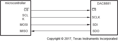
Figure 77 displays a typical serial interface that may be used when connecting the DAC8881 SPI serial interface to a (master) microcontroller. The setup for the interface is as follows: The microcontroller output SPI CLK drives the SCLK pin of the DAC8881, while the DAC8881 SDI pin is driven by the MOSI pin of the microcontroller. The CS pin of the DAC8881 can be asserted from a general program input/output pin of the microcontroller. When data are to be transmitted to the DAC8881, the CS pint is taken low. The data from the microcontroller is then transmitted to the DAC8881, totaling 24 bits latched into the DAC8881 device through the negative edge of SCLK. CS is then brought high after the completed write. The DAC8881 requires its data with the MSB as the first bit received.
DAC8881 Microcontroller_DAC8881.gifFigure 77. Simplified Sample and Hold Circuit