ZHCSHA4B July 2007 – January 2018 DAC8881
PRODUCTION DATA.
- 1 特性
- 2 应用
- 3 说明
- 4 修订历史记录
- 5 Pin Configuration and Functions
- 6 Specifications
-
7 Detailed Description
- 7.1 Overview
- 7.2 Functional Block Diagram
- 7.3 Feature Description
- 7.4 Device Functional Modes
- 8 Application and Implementation
- 9 Power Supply Recommendations
- 10Layout
- 11器件和文档支持
封装选项
机械数据 (封装 | 引脚)
- RGE|24
散热焊盘机械数据 (封装 | 引脚)
- RGE|24
订购信息
8.2.1.1 Design Requirements
The inherent architecture of the DAC8881, which consists of an R-2R architecture, enables great performance in regards to noise and accuracy, but at a cost of large glitch area. Glitch area, also known as glitch impulse area, is defined as the area associated with the overshoot or undershoot created by a code transition, and is generally quantified in Volt-seconds. Different code-to-code transitions produce different levels of glitch impulses. DACs with R-2R architectures produce large glitches during major-carry transitions.
There are two methods that can be used to reduce this glitch area:
- Add an external RC Filter to the output of the DAC.
- The low-pass filter helps attenuate high-frequency glitches that would normally propagate to the DAC output. Best practice is to use a small resistor value, as large resistance develops a large potential drop and reduces the voltage seen at the load. Capacitor values can be determined from the desired cutoff frequency of the low-pass filter, as well as settling time.
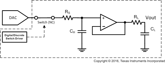
- Another technique is to employ a Sample and Hold (S&H) circuit following the DAC output.
- In its simplest form, the sample and hold circuit can be constructed from the following components: a capacitive element, output buffer, and switch. A schematic of the simplified S&H is shown in Figure 74.
 Figure 74. Simplified Sample and Hold Circuit