ZHCSC70D December   2013  – December 2021 DAC7750 , DAC8750

PRODUCTION DATA  

  1. 特性
  2. 应用
  3. 说明
  4. Revision History
  5. Device Comparison Table
  6. Pin Configuration and Functions
  7. Specifications
    1. 7.1  Absolute Maximum Ratings
    2. 7.2  ESD Ratings
    3. 7.3  Recommended Operating Conditions
    4. 7.4  Thermal Information
    5. 7.5  Electrical Characteristics
    6. 7.6  Electrical Characteristics: AC
    7. 7.7  Timing Requirements: Write Mode
    8. 7.8  Timing Requirements: Readback Mode
    9. 7.9  Timing Diagrams
    10. 7.10 Typical Characteristics
  8. Detailed Description
    1. 8.1 Overview
    2. 8.2 Functional Block Diagram
    3. 8.3 Feature Description
      1. 8.3.1  DAC Architecture
      2. 8.3.2  Current Output Stage
      3. 8.3.3  Internal Reference
      4. 8.3.4  Digital Power Supply
      5. 8.3.5  DAC Clear
      6. 8.3.6  Power-On Reset
      7. 8.3.7  Alarm Detection
      8. 8.3.8  Watchdog Timer
      9. 8.3.9  Frame Error Checking
      10. 8.3.10 User Calibration
      11. 8.3.11 Programmable Slew Rate
    4. 8.4 Device Functional Modes
      1. 8.4.1 Setting Current-Output Ranges
      2. 8.4.2 Current-Setting Resistor
      3. 8.4.3 BOOST Configuration for IOUT
      4. 8.4.4 Filtering The Current Output
      5. 8.4.5 Output Current Monitoring
      6. 8.4.6 HART Interface
        1. 8.4.6.1 Implementing HART in 4-mA to 20-mA Mode
        2. 8.4.6.2 Implementing HART in All Current Output Modes
    5. 8.5 Programming
      1. 8.5.1 Serial Peripheral Interface (SPI)
        1. 8.5.1.1 SPI Shift Register
        2. 8.5.1.2 Write Operation
        3. 8.5.1.3 Read Operation
        4. 8.5.1.4 Stand-Alone Operation
        5. 8.5.1.5 Multiple Devices on the Bus
    6. 8.6 Register Maps
      1. 8.6.1 DACx750 Register Descriptions
        1. 8.6.1.1 Control Register
        2. 8.6.1.2 Configuration Register
        3. 8.6.1.3 DAC Registers
        4. 8.6.1.4 Reset Register
        5. 8.6.1.5 Status Register
  9. Application and Implementation
    1. 9.1 Application Information
      1. 9.1.1 HART Implementation
        1. 9.1.1.1 Using the CAP2 Pin
        2. 9.1.1.2 Using the ISET-R Pin
    2. 9.2 Typical Application
      1. 9.2.1 Design Requirements
      2. 9.2.2 Detailed Design Procedure
      3. 9.2.3 Application Curve
  10. 10Power Supply Recommendations
  11. 11Layout
    1. 11.1 Layout Guidelines
      1. 11.1.1 Thermal Considerations
    2. 11.2 Layout Example
  12. 12Device and Documentation Support
    1. 12.1 Documentation Support
      1. 12.1.1 Related Documentation
    2. 12.2 接收文档更新通知
    3. 12.3 支持资源
    4. 12.4 Trademarks
    5. 12.5 Electrostatic Discharge Caution
    6. 12.6 术语表
  13. 13Mechanical, Packaging, and Orderable Information

封装选项

机械数据 (封装 | 引脚)
散热焊盘机械数据 (封装 | 引脚)
订购信息

Using the CAP2 Pin

The first method to implement HART is to couple the signal through the CAP2 pin, as shown in Figure 9-1.
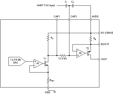
GUID-CC7C967F-A9BC-4327-AFEF-31E9C4376B30-low.gifFigure 9-1 Implementing HART on IOUT Using the CAP2 Pin

In Figure 9-1, R3 is nominally 40 Ω, and R2 depends on the current output range (set by the RANGE bits), described as follows:

  • 4-mA to 20-mA range: R2 = 2.4 kΩ (typical)
  • 0-mA to 20-mA range: R2 = 3 kΩ (typical)
  • 0-mA to 24-mA range: R2 = 3.6 kΩ (typical)

The purpose of the 12.5-kΩ resistor is to create a filter when CAP1 and CAP2 are used.

To insert the external HART signal on the CAP2 pin, an external ac-coupling capacitor is typically connected to CAP2. The high-pass filter 3-dB frequency is determined by the resistive impedance looking into
CAP2 (R2 + 12.5 kΩ) and the coupling-capacitor value. The 3-dB frequency is 1 / (2 × π × [R2 + 12.5 kΩ] × [Coupling Capacitor Value]).

When the input HART frequency is greater than the 3-dB frequency, the ac signal is seen at the plus input of amplifier A2, and is therefore seen across the 40-Ω resistor. To generate a 1-mA signal on the output therefore requires a 40-mV peak-to-peak signal on CAP2. Most HART modems do not output a 40-mV signal; therefore, a capacitive divider is used in Figure 9-1 to attenuate the FSK signal from the modem. In Figure 9-1, the high-pass cutoff frequency is 1 / (2 × π × [R2+ 12.5 kΩ] × [C1 + C2]). There is one disadvantage to this approach: if the AVDD supply is not clean, any ripple on the supply could couple into the device.