ZHCSC70D December   2013  – December 2021 DAC7750 , DAC8750

PRODUCTION DATA  

  1. 特性
  2. 应用
  3. 说明
  4. Revision History
  5. Device Comparison Table
  6. Pin Configuration and Functions
  7. Specifications
    1. 7.1  Absolute Maximum Ratings
    2. 7.2  ESD Ratings
    3. 7.3  Recommended Operating Conditions
    4. 7.4  Thermal Information
    5. 7.5  Electrical Characteristics
    6. 7.6  Electrical Characteristics: AC
    7. 7.7  Timing Requirements: Write Mode
    8. 7.8  Timing Requirements: Readback Mode
    9. 7.9  Timing Diagrams
    10. 7.10 Typical Characteristics
  8. Detailed Description
    1. 8.1 Overview
    2. 8.2 Functional Block Diagram
    3. 8.3 Feature Description
      1. 8.3.1  DAC Architecture
      2. 8.3.2  Current Output Stage
      3. 8.3.3  Internal Reference
      4. 8.3.4  Digital Power Supply
      5. 8.3.5  DAC Clear
      6. 8.3.6  Power-On Reset
      7. 8.3.7  Alarm Detection
      8. 8.3.8  Watchdog Timer
      9. 8.3.9  Frame Error Checking
      10. 8.3.10 User Calibration
      11. 8.3.11 Programmable Slew Rate
    4. 8.4 Device Functional Modes
      1. 8.4.1 Setting Current-Output Ranges
      2. 8.4.2 Current-Setting Resistor
      3. 8.4.3 BOOST Configuration for IOUT
      4. 8.4.4 Filtering The Current Output
      5. 8.4.5 Output Current Monitoring
      6. 8.4.6 HART Interface
        1. 8.4.6.1 Implementing HART in 4-mA to 20-mA Mode
        2. 8.4.6.2 Implementing HART in All Current Output Modes
    5. 8.5 Programming
      1. 8.5.1 Serial Peripheral Interface (SPI)
        1. 8.5.1.1 SPI Shift Register
        2. 8.5.1.2 Write Operation
        3. 8.5.1.3 Read Operation
        4. 8.5.1.4 Stand-Alone Operation
        5. 8.5.1.5 Multiple Devices on the Bus
    6. 8.6 Register Maps
      1. 8.6.1 DACx750 Register Descriptions
        1. 8.6.1.1 Control Register
        2. 8.6.1.2 Configuration Register
        3. 8.6.1.3 DAC Registers
        4. 8.6.1.4 Reset Register
        5. 8.6.1.5 Status Register
  9. Application and Implementation
    1. 9.1 Application Information
      1. 9.1.1 HART Implementation
        1. 9.1.1.1 Using the CAP2 Pin
        2. 9.1.1.2 Using the ISET-R Pin
    2. 9.2 Typical Application
      1. 9.2.1 Design Requirements
      2. 9.2.2 Detailed Design Procedure
      3. 9.2.3 Application Curve
  10. 10Power Supply Recommendations
  11. 11Layout
    1. 11.1 Layout Guidelines
      1. 11.1.1 Thermal Considerations
    2. 11.2 Layout Example
  12. 12Device and Documentation Support
    1. 12.1 Documentation Support
      1. 12.1.1 Related Documentation
    2. 12.2 接收文档更新通知
    3. 12.3 支持资源
    4. 12.4 Trademarks
    5. 12.5 Electrostatic Discharge Caution
    6. 12.6 术语表
  13. 13Mechanical, Packaging, and Orderable Information

封装选项

机械数据 (封装 | 引脚)
散热焊盘机械数据 (封装 | 引脚)
订购信息

BOOST Configuration for IOUT

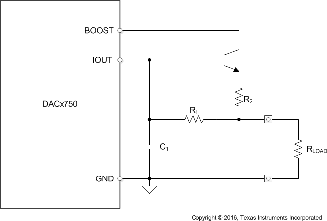
Figure 8-5 illustrates an external NPN transistor used to reduce power dissipation on the die. Most of the load current flows through the NPN transistor with a small amount flowing through the on-chip PMOS transistor based on the gain of the NPN transistor. This configuration reduces the temperature induced drift on the die and internal reference and is an option for use cases at the extreme end of the supply, load current, and ambient temperature ranges.

The inclusion of the bipolar junction transistor (BJT) adds an additional open loop gain to internal amplifier A2 (see Figure 8-2) and thus, can cause possible instability. Adding series emitter resistor R2 decreases the gain of the stage created by the BJT and internal R3 resistor (see Figure 8-2) especially for cases where RLOAD is a short or a very small load, such as a multimeter. Recommended values for R1, R2, and C1 in this circuit are 1 kΩ, 30 Ω and 22 nF, respectively. An equivalent solution is to place R2 (with a recommended value of 3 kΩ instead of 30 Ω) in series with the base of the transistor instead of the configuration provided in Figure 8-5. Note that there is some gain error introduced by this configuration; see Figure 7-14, Figure 7-15 and Figure 7-16. Use the internal transistor in most cases because the values in Section 7.5 are based on the configuration with the internal on-chip PMOS transistor.
GUID-9786DD0C-78A6-4DE1-9F0A-CB16AD18FB05-low.gifFigure 8-5 Boost Mode Configuration