ZHCSJ19E november 2018 – august 2023 DAC60501 , DAC70501 , DAC80501
PRODUCTION DATA
- 1
- 1 特性
- 2 应用
- 3 说明
- 4 Revision History
- 5 Device Comparison Table
- 6 Pin Configuration and Functions
-
7 Specifications
- 7.1 Absolute Maximum Ratings
- 7.2 ESD Ratings
- 7.3 Recommended Operating Conditions
- 7.4 Thermal Information
- 7.5 Electrical Characteristics
- 7.6 Timing Requirements: SPI Mode
- 7.7 Timing Requirements: I2C Standard Mode
- 7.8 Timing Requirements: I2C Fast Mode
- 7.9 Timing Requirements: I2C Fast-Mode Plus
- 7.10 Timing Diagrams
- 7.11 Typical Characteristics
- 8 Detailed Description
- 9 Application and Implementation
- 10Device and Documentation Support
- 11Mechanical, Packaging, and Orderable Information
8.3.1.1 DAC Transfer Function
The input data writes to the individual DAC data registers in straight binary format. After a power-on or a reset event, all DAC registers are set to zero code (DACx0501Z devices) or midscale code (DACx0501M devices). The DAC transfer function is shown by Equation 1.
Equation 1. 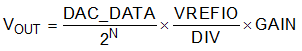
where:
- N = resolution in bits = either 12 (DAC60501), 14 (DAC70501) or 16 (DAC80501).
- DAC_DATA = decimal equivalent of the binary code that is loaded to the DAC register (address 8h). DAC_DATA ranges from 0 to 2N – 1.
- VREFIO = DAC reference voltage at the VREFIO pin. Either VREFIO from the internal 2.5-V reference or VREFIO from an external reference.
- DIV = 1 (default) or 2, as set by the REF-DIV bit in the GAIN register (address 4h).
- GAIN = 1 or 2 (default), as set by the BUFF-GAIN bit in the GAIN register (address 4h).