ZHCSEI7B December   2015  – December 2017 CSD95377Q4M

PRODUCTION DATA.  

  1. 特性
  2. 应用
  3. 说明
    1.     Device Images
  4. 修订历史记录
  5. Pin Configuration and Functions
    1.     Pin Functions
  6. Specifications
    1. 6.1 Absolute Maximum Ratings
    2. 6.2 ESD Ratings
    3. 6.3 Recommended Operating Conditions
    4. 6.4 Thermal Information
    5. 6.5 Electrical Characteristics
  7. Detailed Description
    1. 7.1 Overview
    2. 7.2 Functional Block Diagram
    3. 7.3 Feature Description
      1. 7.3.1 Powering CSD95377Q4M and Gate Drivers
      2. 7.3.2 Undervoltage Lockout (UVLO) Protection
      3. 7.3.3 PWM Pin
      4. 7.3.4 SKIP# Pin
        1. 7.3.4.1 Zero Crossing (ZX) Operation
      5. 7.3.5 Integrated Boost-Switch
    4. 7.4 Device Functional Modes
  8. Application and Implementation
    1. 8.1 Application Information
    2. 8.2 Typical Application
      1. 8.2.1 Application Curves
    3. 8.3 System Example
      1. 8.3.1 Power Loss Curves
      2. 8.3.2 Safe Operating Area (SOA) Curves
      3. 8.3.3 Normalized Curves
      4. 8.3.4 Calculating Power Loss and SOA
        1. 8.3.4.1 Design Example
        2. 8.3.4.2 Calculating Power Loss
        3. 8.3.4.3 Calculating SOA Adjustments
  9. Layout
    1. 9.1 Layout Guidelines
      1. 9.1.1 Recommended PCB Design Overview
      2. 9.1.2 Electrical Performance
    2. 9.2 Layout Example
    3. 9.3 Thermal Considerations
  10. 10器件和文档支持
    1. 10.1 接收文档更新通知
    2. 10.2 社区资源
    3. 10.3 商标
    4. 10.4 静电放电警告
    5. 10.5 Glossary
  11. 11机械、封装和可订购信息
    1. 11.1 机械制图
    2. 11.2 建议印刷电路板 (PCB) 焊盘图案
    3. 11.3 建议模版开口

封装选项

请参考 PDF 数据表获取器件具体的封装图。

机械数据 (封装 | 引脚)
  • DPC|8
散热焊盘机械数据 (封装 | 引脚)
订购信息

Calculating SOA Adjustments

  • SOA adjustment for switching frequency ≈ 0.3°C (Figure 8)
  • SOA adjustment for input voltage ≈ –0.12°C (Figure 9)
  • SOA adjustment for output voltage ≈ 0.62°C (Figure 10)
  • SOA adjustment for output inductor ≈ 0.25°C (Figure 11)
  • Final calculated SOA adjustment = 0.3 + (–0.12) + 0.62 + 0.25 ≈ 1.05°C
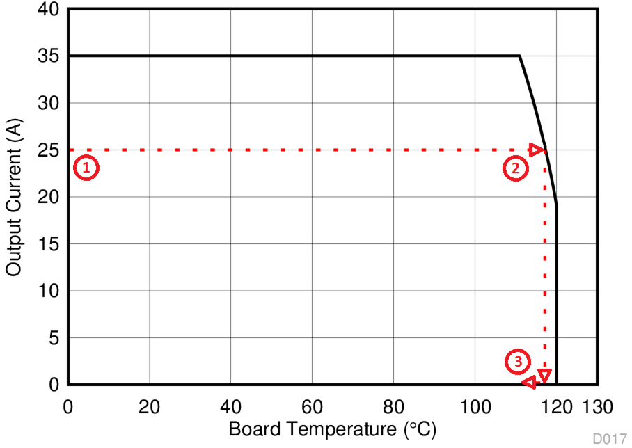
CSD95377Q4M D017_SLPS584.gifFigure 15. Power Stage CSD95377Q4M SOA

In the previous design example, the estimated power loss of the CSD95377Q4M would increase to 3.97 W. In addition, the maximum allowable board and/or ambient temperature would have to decrease by 1.05°C. Figure 15 graphically shows how the SOA curve would be adjusted accordingly.

  1. Start by drawing a horizontal line from the application current to the SOA curve.
  2. Draw a vertical line from the SOA curve intercept down to the board/ambient temperature.
  3. Adjust the SOA board/ambient temperature by subtracting the temperature adjustment value.

In the design example, the SOA temperature adjustment yields a reduction in allowable board/ambient temperature of 1.05°C. In the event the adjustment value is a negative number, subtracting the negative number would yield an increase in allowable board and ambient temperature.