ZHCSEI7B December   2015  – December 2017 CSD95377Q4M

PRODUCTION DATA.  

  1. 特性
  2. 应用
  3. 说明
    1.     Device Images
  4. 修订历史记录
  5. Pin Configuration and Functions
    1.     Pin Functions
  6. Specifications
    1. 6.1 Absolute Maximum Ratings
    2. 6.2 ESD Ratings
    3. 6.3 Recommended Operating Conditions
    4. 6.4 Thermal Information
    5. 6.5 Electrical Characteristics
  7. Detailed Description
    1. 7.1 Overview
    2. 7.2 Functional Block Diagram
    3. 7.3 Feature Description
      1. 7.3.1 Powering CSD95377Q4M and Gate Drivers
      2. 7.3.2 Undervoltage Lockout (UVLO) Protection
      3. 7.3.3 PWM Pin
      4. 7.3.4 SKIP# Pin
        1. 7.3.4.1 Zero Crossing (ZX) Operation
      5. 7.3.5 Integrated Boost-Switch
    4. 7.4 Device Functional Modes
  8. Application and Implementation
    1. 8.1 Application Information
    2. 8.2 Typical Application
      1. 8.2.1 Application Curves
    3. 8.3 System Example
      1. 8.3.1 Power Loss Curves
      2. 8.3.2 Safe Operating Area (SOA) Curves
      3. 8.3.3 Normalized Curves
      4. 8.3.4 Calculating Power Loss and SOA
        1. 8.3.4.1 Design Example
        2. 8.3.4.2 Calculating Power Loss
        3. 8.3.4.3 Calculating SOA Adjustments
  9. Layout
    1. 9.1 Layout Guidelines
      1. 9.1.1 Recommended PCB Design Overview
      2. 9.1.2 Electrical Performance
    2. 9.2 Layout Example
    3. 9.3 Thermal Considerations
  10. 10器件和文档支持
    1. 10.1 接收文档更新通知
    2. 10.2 社区资源
    3. 10.3 商标
    4. 10.4 静电放电警告
    5. 10.5 Glossary
  11. 11机械、封装和可订购信息
    1. 11.1 机械制图
    2. 11.2 建议印刷电路板 (PCB) 焊盘图案
    3. 11.3 建议模版开口

封装选项

请参考 PDF 数据表获取器件具体的封装图。

机械数据 (封装 | 引脚)
  • DPC|8
散热焊盘机械数据 (封装 | 引脚)
订购信息

Application Curves

TJ = 125°C, unless stated otherwise.
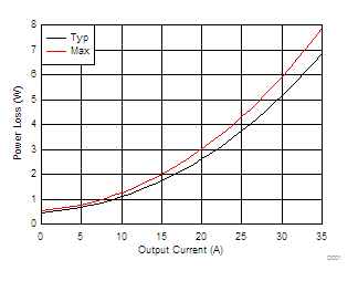
CSD95377Q4M D001_SLPS584.gif
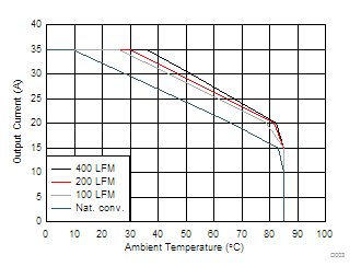
VIN = 12 V VDD = 5 V VOUT = 1.8 V
ƒSW = 500 kHz LOUT = 0.29 µH
Figure 4. Power Loss vs Output Current
CSD95377Q4M D003_SLPS584.gif
VIN = 12 V VDD = 5 V VOUT = 1.8 V
ƒSW = 500 kHz LOUT = 0.29 µH
Figure 6. Safe Operating Area – PCB Horizontal Mount (1)
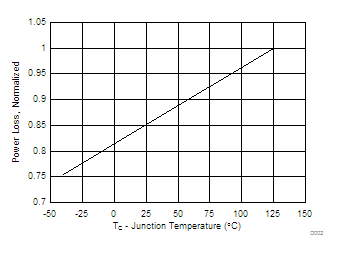
CSD95377Q4M D002_SLPS584.gif
VIN = 12 V VDD = 5 V VOUT = 1.8 V
ƒSW = 500 kHz LOUT = 0.29 µH
Figure 5. Power Loss vs Temperature
CSD95377Q4M D004_SLPS584.gif
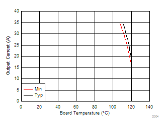
VIN = 12 V VDD = 5 V VOUT = 1.8 V
ƒSW = 500 kHz LOUT = 0.29 µH
Figure 7. Typical Safe Operating Area (1)
  1. The typical CSD95377Q4M system characteristic curves are based on measurements made on a PCB design with dimensions of 4 in (W) × 3.5 in (L) × 0.062 in (T) and 6 copper layers of 1-oz copper thickness. See System Example for detailed explanation.
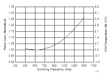
CSD95377Q4M D005_SLPS584.gif
VIN = 12 V VDD = 5 V VOUT = 1.8 V
IOUT = 35 A LOUT = 0.29 µH
Figure 8. Normalized Power Loss vs Frequency
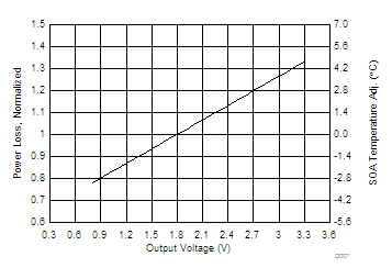
CSD95377Q4M D007_SLPS584.gif
VIN = 12 V VDD = 5 V IOUT = 35 A
ƒSW = 500 kHz LOUT = 0.29 µH
Figure 10. Normalized Power Loss vs Output Voltage
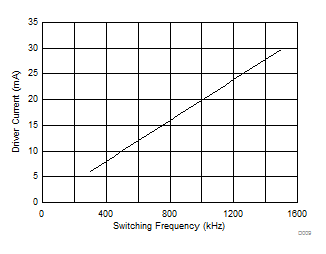
CSD95377Q4M D009_SLPS584.gif
VIN = 12 V VDD = 5 V IOUT = 35 A
LOUT = 0.29 µH VOUT = 1.8 V
Figure 12. Driver Current vs Frequency
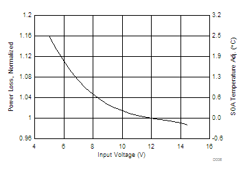
CSD95377Q4M D006_SLPS584.gif
IOUT = 35 A VDD = 5 V VOUT = 1.8 V
ƒSW = 500 kHz LOUT = 0.29 µH
Figure 9. Normalized Power Loss vs Input Voltage
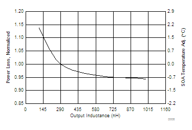
CSD95377Q4M D008_SLPS584.gif
VIN = 12 V VDD = 5 V IOUT = 35 A
ƒSW = 500 kHz VOUT = 1.8 V
Figure 11. Normalized Power Loss vs Output Inductance
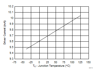
CSD95377Q4M D010_SLPS584.gif
VIN = 12 V VDD = 5 V VOUT = 1.8 V
IOUT = 35 A LOUT = 0.29 µH
Figure 13. Driver Current vs Temperature