ZHCSGV7F July 2017 – January 2024 CDCI6214
PRODUCTION DATA
- 1
- 1 特性
- 2 应用
- 3 说明
- 4 Device Comparison
- 5 Pin Configuration and Functions
-
6 Specifications
- 6.1 Absolute Maximum Ratings
- 6.2 ESD Ratings
- 6.3 Recommended Operating Conditions
- 6.4 Thermal Information
- 6.5 EEPROM Characteristics
- 6.6 Reference Input, Single-Ended and Differential Mode Characteristics (REFP, REFN, FB_P, FB_N)
- 6.7 Reference Input, Crystal Mode Characteristics (XIN, XOUT)
- 6.8 General-Purpose Input and Output Characteristics (GPIO[4:1], SYNC/RESETN)
- 6.9 Triple Level Input Characteristics (EEPROMSEL, REFSEL)
- 6.10 Reference Mux Characteristics
- 6.11 Phase-Locked Loop Characteristics
- 6.12 Closed-Loop Output Jitter Characteristics
- 6.13 Output Mux Characteristics
- 6.14 LVCMOS Output Characteristics
- 6.15 HCSL Output Characteristics
- 6.16 LVDS DC-Coupled Output Characteristics
- 6.17 Programmable Differential AC-Coupled Output Characteristics
- 6.18 Output Skew and Delay Characteristics
- 6.19 Output Synchronization Characteristics
- 6.20 Timing Characteristics
- 6.21 I2C-Compatible Serial Interface Characteristics (SDA/GPIO2, SCL/GPIO3)
- 6.22 Timing Requirements, I2C-Compatible Serial Interface (SDA/GPIO2, SCL/GPIO3)
- 6.23 Power Supply Characteristics
- 6.24 Typical Characteristics
- 7 Parameter Measurement Information
-
8 Detailed Description
- 8.1 Overview
- 8.2 Functional Block Diagram
- 8.3 Feature Description
- 8.4 Device Functional Modes
- 8.5 Programming
- 9 Application and Implementation
- 10Register Maps
- 11Device and Documentation Support
- 12Revision History
- 13Mechanical, Packaging, and Orderable Information
8.3.2 Phase-Locked Loop
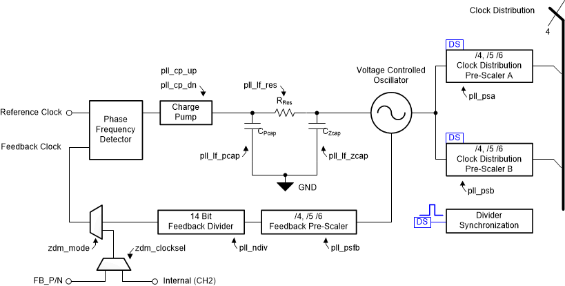
The CDCI6214 contains a fully integrated phase-locked loop circuit. The error between a reference phase and an internal feedback phase is compared at the phase-frequency-detector. The comparison result is fed to a charge pump that is connected to an integrated loop filter. The control voltage resulting from the loop filter tunes an internal voltage-controlled oscillator (VCO). The frequency of the VCO is fed through a pre-scaler feedback divider (PSFB) and another feedback divider back to the PFD.
The PLL closed-loop bandwidth is configurable using registers PLL0, PLL1, and PLL2.
- Integer PLL
- PFD operates 1 MHz to 100 MHz
- Live Lock-Detector provides PLL lock status on status pin and bit lock_det (there is an additional sticky bit unlock_s)
- Integrated selectable loop filter components
- For 25-MHz PFD bandwidths between 100 kHz and 3000 kHz can be achieved to optimize PLL to input reference
- Voltage-Controlled Oscillator (VCO) tuning range of 2400 to 2800 MHz
- VCO is compatible to 0.5% spread spectrum (SSC) references at 100 MHz.
 Figure 8-3 Phase-Locked Loop Circuit
| fVCO in MHz(1) | fPFD in MHz | BW in MHz | Phase Margin in ° | Damping Factor | ICP in mA | CPcap IN pF | RRes IN kΩ | CZcap IN pF |
|---|---|---|---|---|---|---|---|---|
| pll_cp_up(2) | pll_lf_pcap | pll_lf_res | pll_lf_zcap | |||||
| 2400 | 25 | 0.51 | 67 | 0.9 | 2.0 | 17.5 | 2.5 | 450 |
| 2400 | 50 | 0.97 | 67 | 1.3 | 2.0 | 17.5 | 2.5 | 450 |
| 2400 | 100 | 1.41 | 68 | 1.2 | 2.4 | 17.5 | 1.5 | 450 |
| 2457.6 | 61.44 | 1.04 | 67 | 1.4 | 1.8 | 17.5 | 2.5 | 450 |
| 2500 | 25 | 0.49 | 67 | 0.9 | 2.0 | 17.5 | 2.5 | 450 |
| 2500 | 50 | 0.93 | 68 | 1.3 | 2.0 | 17.5 | 2.5 | 450 |
| 2680 | 67 | 0.38 | 67 | 1.3 | 0.2 | 19.5 | 5.5 | 480 |
| 2688 | 48 | 0.93 | 68 | 1.3 | 1.5 | 17.5 | 2.5 | 480 |
| 2688 | 96 | 0.36 | 67 | 1.0 | 0.2 | 19.5 | 3.5 | 480 |
| 2800 | 50 | 1.00 | 68 | 1.0 | 2.6 | 17.5 | 1.5 | 450 |
| 2800 | 100 | 1.00 | 68 | 1.0 | 1.3 | 17.5 | 1.5 | 450 |