ZHCSGV7F July 2017 – January 2024 CDCI6214
PRODUCTION DATA
- 1
- 1 特性
- 2 应用
- 3 说明
- 4 Device Comparison
- 5 Pin Configuration and Functions
-
6 Specifications
- 6.1 Absolute Maximum Ratings
- 6.2 ESD Ratings
- 6.3 Recommended Operating Conditions
- 6.4 Thermal Information
- 6.5 EEPROM Characteristics
- 6.6 Reference Input, Single-Ended and Differential Mode Characteristics (REFP, REFN, FB_P, FB_N)
- 6.7 Reference Input, Crystal Mode Characteristics (XIN, XOUT)
- 6.8 General-Purpose Input and Output Characteristics (GPIO[4:1], SYNC/RESETN)
- 6.9 Triple Level Input Characteristics (EEPROMSEL, REFSEL)
- 6.10 Reference Mux Characteristics
- 6.11 Phase-Locked Loop Characteristics
- 6.12 Closed-Loop Output Jitter Characteristics
- 6.13 Output Mux Characteristics
- 6.14 LVCMOS Output Characteristics
- 6.15 HCSL Output Characteristics
- 6.16 LVDS DC-Coupled Output Characteristics
- 6.17 Programmable Differential AC-Coupled Output Characteristics
- 6.18 Output Skew and Delay Characteristics
- 6.19 Output Synchronization Characteristics
- 6.20 Timing Characteristics
- 6.21 I2C-Compatible Serial Interface Characteristics (SDA/GPIO2, SCL/GPIO3)
- 6.22 Timing Requirements, I2C-Compatible Serial Interface (SDA/GPIO2, SCL/GPIO3)
- 6.23 Power Supply Characteristics
- 6.24 Typical Characteristics
- 7 Parameter Measurement Information
-
8 Detailed Description
- 8.1 Overview
- 8.2 Functional Block Diagram
- 8.3 Feature Description
- 8.4 Device Functional Modes
- 8.5 Programming
- 9 Application and Implementation
- 10Register Maps
- 11Device and Documentation Support
- 12Revision History
- 13Mechanical, Packaging, and Orderable Information
8.5.2 EEPROM Access
The EEPROM word write access time is typically 8 ms. The EEPROM_BUSY signal indicates when the EEPROM is busy and can be observed as a status signal on a GPIO pin to optimally time the writes (for example, in gpio4_output_sel).
There are two methods to write into the internal EEPROM:
- Register Commit
- EEPROM Direct Access
Use the following steps to bring the device into a known state and be able to conduct the programming:
- Power down all device supplies
- Apply RESETN=LOW.
- Apply REFSEL=MID (leave tri-stated).
- Apply EEPROMSEL=MID (leave tri-stated).
- Apply 1.8 V/2.5 V/3.3 V to all device supplies. When device operation is not required, only apply 1.8 V/2.5V/3.3 V to VDDREF.
- Apply RESETN=HIGH.
- Use the I2C interface to configure the device using target address 0x74. See Table 8-12 for more details.
In the Register Commit flow all bits from the device registers are copied into the EEPROM. The recommended flow is:
- Pre-configure the device as desired, except the serial interface using mode.
- Write 1 to recal to calibrate the VCO in this operation mode.
- Select the EEPROM page, to copy the register settings into, using regcommit_page.
- Unlock the EEPROM for write access with ee_lock = 0x5
- Start the commit operation by writing a 1 to regcommit
- Force a CRC update by writing a 1 to update_crc.
- Read back the calculated CRC in nvmlcrc.
- Store the read CRC value in the EEPROM by writing 0x3F to nvm_wr_addr and then the CRC value to nvm_wr_data.
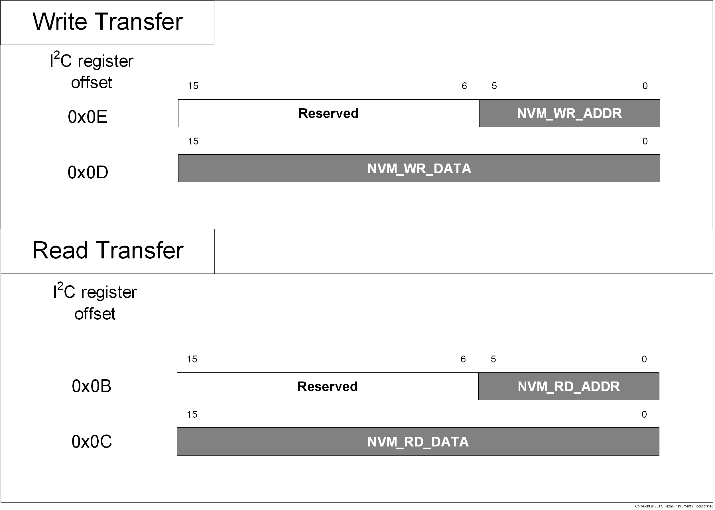
In the EEPROM Direct Access flow the EEPROM words are directly accessed using the address and the data bit-fields. The recommended flow is:
- Prepare an EEPROM image consisting of 64 words.
- Unlock the EEPROM for write access with ee_lock = 0x5
- Write the initial address offset to the address bit-field. Write a 0x00 to nvm_wr_addr.
- Loop through the EEPROM image from address 0 to 63 by writing each word from the image to nvm_wr_data. The EEPROM word address is automatically incremented by every write access to nvm_wr_data.
- The EEPROM read is similar to EEPROM write. First write 0x00 to nvm_rd_addr, then loop through all bytes by reading from nvm_rd_data. The EEPROM word address is automatically incremented by every write access to nvm_rd_data.
 Figure 8-12 EEPROM Direct Access Using I2C