ZHCSGV7F July 2017 – January 2024 CDCI6214
PRODUCTION DATA
- 1
- 1 特性
- 2 应用
- 3 说明
- 4 Device Comparison
- 5 Pin Configuration and Functions
-
6 Specifications
- 6.1 Absolute Maximum Ratings
- 6.2 ESD Ratings
- 6.3 Recommended Operating Conditions
- 6.4 Thermal Information
- 6.5 EEPROM Characteristics
- 6.6 Reference Input, Single-Ended and Differential Mode Characteristics (REFP, REFN, FB_P, FB_N)
- 6.7 Reference Input, Crystal Mode Characteristics (XIN, XOUT)
- 6.8 General-Purpose Input and Output Characteristics (GPIO[4:1], SYNC/RESETN)
- 6.9 Triple Level Input Characteristics (EEPROMSEL, REFSEL)
- 6.10 Reference Mux Characteristics
- 6.11 Phase-Locked Loop Characteristics
- 6.12 Closed-Loop Output Jitter Characteristics
- 6.13 Output Mux Characteristics
- 6.14 LVCMOS Output Characteristics
- 6.15 HCSL Output Characteristics
- 6.16 LVDS DC-Coupled Output Characteristics
- 6.17 Programmable Differential AC-Coupled Output Characteristics
- 6.18 Output Skew and Delay Characteristics
- 6.19 Output Synchronization Characteristics
- 6.20 Timing Characteristics
- 6.21 I2C-Compatible Serial Interface Characteristics (SDA/GPIO2, SCL/GPIO3)
- 6.22 Timing Requirements, I2C-Compatible Serial Interface (SDA/GPIO2, SCL/GPIO3)
- 6.23 Power Supply Characteristics
- 6.24 Typical Characteristics
- 7 Parameter Measurement Information
-
8 Detailed Description
- 8.1 Overview
- 8.2 Functional Block Diagram
- 8.3 Feature Description
- 8.4 Device Functional Modes
- 8.5 Programming
- 9 Application and Implementation
- 10Register Maps
- 11Device and Documentation Support
- 12Revision History
- 13Mechanical, Packaging, and Orderable Information
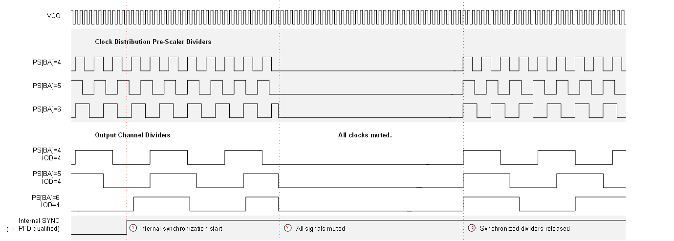
8.3.6 Divider Synchronization - SYNC
The output dividers can be reset in a deterministic way. This can be achieved using the sync bit or the pin 8 configured for SYNC function using gpio0_input_sel and gpio0_dir_sel. The level of the pin is qualified internally using the reference frequency at the PFD. A low level will mute the outputs. A high level will synchronously release all output dividers to operation, so that all outputs share a common rising edge, see Figure 8-8. The first rising edge can be individually delayed in steps of the respective pre-scaler period, up to 32 cycles using ch1_sync_delay. This allows to compensate external delays like routing mismatch, cables or inherent delays introduced by logic gates in an FPGA design. Each channel can be included or excluded from the SYNC process using ch1_sync_en. (2)(3)
For a deterministic behaviour over power-cycles seen from input to output the reference divider must be set to 1. It should not divide the reference clock nor should the reference doubler be used.
 Figure 8-8 Divider Synchronization
| VCO FREQUENCY IN MHz | PRE-SCALER STEP IN ns | ||
|---|---|---|---|
| /4 | /5 | /6 | |
| 2400 | 1.67 | 2.08 | 2.50 |
| 2457.6 | 1.63 | 2.03 | 2.44 |
| 2500 | 1.60 | 2.00 | 2.40 |
| 2800 | 1.43 | 1.79 | 2.14 |