ZHCSK34B July 2020 – October 2021 CDCE6214-Q1
PRODUCTION DATA
- 1 特性
- 2 应用
- 3 说明
- 4 Revision History
- 5 说明(续)
- 6 Pin Configuration and Functions
-
7 Specifications
- 7.1 Absolute Maximum Ratings
- 7.2 ESD Ratings
- 7.3 Recommended Operating Conditions
- 7.4 Thermal Information
- 7.5 EEPROM Characteristics
- 7.6 Reference Input, Single-Ended Characteristics
- 7.7 Reference Input, Differential Characteristics
- 7.8 Reference Input, Crystal Mode Characteristics
- 7.9 General-Purpose Input Characteristics
- 7.10 Triple Level Input Characteristics
- 7.11 Logic Output Characteristics
- 7.12 Phase Locked Loop Characteristics
- 7.13 Closed-Loop Output Jitter Characteristics
- 7.14 Input and Output Isolation
- 7.15 Buffer Mode Characteristics
- 7.16 PCIe Spread Spectrum Generator
- 7.17 LVCMOS Output Characteristics
- 7.18 LP-HCSL Output Characteristics
- 7.19 LVDS Output Characteristics
- 7.20 Output Synchronization Characteristics
- 7.21 Power-On Reset Characteristics
- 7.22 I2C-Compatible Serial Interface Characteristics
- 7.23 Timing Requirements, I2C-Compatible Serial Interface
- 7.24 Power Supply Characteristics
- 7.25 Typical Characteristics
- 8 Parameter Measurement Information
- 9 Detailed Description
- 10Application and Implementation
- 11Power Supply Recommendations
- 12Layout
- 13Device and Documentation Support
- 14Mechanical, Packaging, and Orderable Information
9.3.2.2 Spread Spectrum Clocking
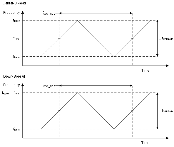
The energy of the harmonics from the rectangular clock signal can be spread over a certain frequency range. This frequency deviation leads to lowered average amplitude of the harmonics. This can help to mitigate electromagnetic interference (EMI) challenges in a system when the receiver supports this mode of operation. The modulation shape is triangular.
The SSC clock is generated through the fractional-N PLL. When SSC is enabled, SSC clock is available on all clock sourced from the PLL. Reference clock or PFD clock is available on the OUT1–OUT4 pins.
Down spread and center spread are supported. The following modes are supported.
- PFD frequencies: Either 25 MHz or 50 MHz.
- Down spread: –0.25% and ±0.5%
- Center spread: ±0.25% and ±0.5%
Using these pre-configured settings, fmod of 31.5 kHz is synthesized for 100-MHz output clock.
 Figure 9-3 Spread Spectrum Clock
| R41[15] - SSC_EN | R42[5] - SSC_TYPE | R42[3:1] - SSC_SEL | DESCRIPTION |
|---|---|---|---|
| 0h | X | X | No SSC modulation at output |
| 1h | 0h | X | Down spread SSC modulation. SSC spread is determined by ssc_sel |
| 1h | 1h | X | Center spread SSC modulation. SSC spread is determined by ssc_sel |
| 1h | X | 0h | 25-MHz PFD, +/- 0.25% for Center spread, -0.25% for Down spread. |
| 1h | X | 1h | 25-MHz PFD, +/- 0.50% for Center spread, -0.50% for Down spread. |
| 1h | X | 2h | 50-MHz PFD, +/- 0.25% for Center spread, -0.25% for Down spread. |
| 1h | X | 3h | 50-MHz PFD, +/- 0.50% for Center spread, -0.50% for Down spread. |
| 1h | X | 4h-7h | Do not use |
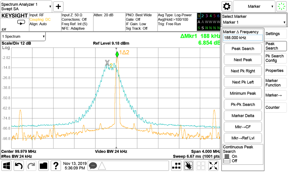
 Figure 9-4 100 MHz With - 0.25% Down Spread With and Without Trace
 Figure 9-6 100 MHz With - 0.5% Down Spread With and Without Trace
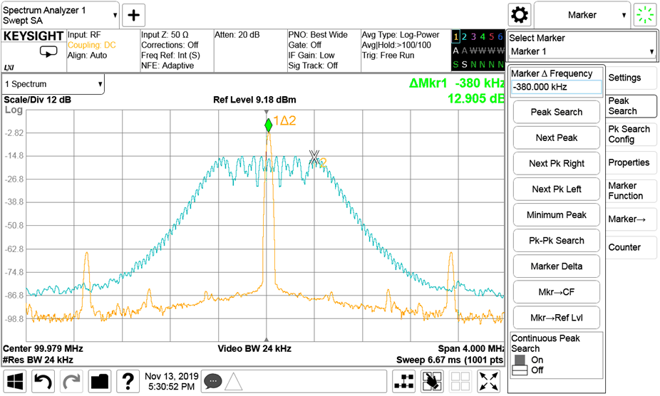
 Figure 9-5 100 MHz With +/- 0.25% Center Spread With and Without Trace
 Figure 9-7 100 MHz With +/- 0.5% Center Spread With and Without Trace
| NO. | CLASS | DATA RATE | ARCHITECTURE | MEASURED PNA METHOD | MEASURED SCOPE METHOD | SPEC LIMIT | RESULT |
|---|---|---|---|---|---|---|---|
| 1 | Gen4 | 16 Gb/s | CC | 195 fs | 260 fs | 500 fs | PASS |
| 2 | Gen4 | 16 Gb/s | SRIS | - | 490 fs | 500 fs | PASS |
| 3 | Gen5 | 32 Gb/s | CC | 87 fs | 111 fs | 150 fs | PASS |
| 4 | Gen5 | 32 Gb/s | SRIS | - | 157 fs | * | * |