ZHCSF60K June 2016 – July 2020 BQ77904 , BQ77905
PRODUCTION DATA
- 1 特性
- 2 应用
- 3 说明
- 4 Revision History
- 5 Device Comparison
- 6 Pin Configuration and Functions
- 7 Specifications
-
8 Detailed Description
- 8.1 Overview
- 8.2 Functional Block Diagram
- 8.3
Feature Description
- 8.3.1 Protection Summary
- 8.3.2
Fault Operation
- 8.3.2.1 Operation in OV
- 8.3.2.2 Operation in UV
- 8.3.2.3 Operation in OW
- 8.3.2.4 Operation in OCD1
- 8.3.2.5 Operation in OCD2
- 8.3.2.6 Operation in SCD
- 8.3.2.7 Overcurrent Recovery Timer
- 8.3.2.8 Load Removal Detection
- 8.3.2.9 Load Removal Detection in UV
- 8.3.2.10 Operation in OTC
- 8.3.2.11 Operation in OTD
- 8.3.2.12 Operation in UTC
- 8.3.2.13 Operation in UTD
- 8.3.3 Protection Response and Recovery Summary
- 8.3.4 Configuration CRC Check and Comparator Built-In-Self-Test
- 8.3.5 Fault Detection Method
- 8.3.6 State Comparator
- 8.3.7 DSG FET Driver Operation
- 8.3.8 CHG FET Driver Operation
- 8.3.9 External Override of CHG and DSG Drivers
- 8.3.10 Configuring 3-S, 4-S, or 5-S Mode
- 8.3.11 Stacking Implementations
- 8.3.12 Zero-Volt Battery Charging Inhibition
- 8.4 Device Functional Modes
- 9 Application and Implementation
- 10Power Supply Recommendations
- 11Layout
- 12Device and Documentation Support
- 13Mechanical, Packaging, and Orderable Information
8.3.1 Protection Summary
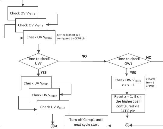
The BQ77904 and BQ77905 have two comparators. Both are time multiplexed to detect all protection fault conditions. Each of the comparators runs on a time-multiplexed schedule and cycles through the assigned protection-fault checks. Comparator 1 checks for OV, UV, and OW protection faults. Comparator 2 checks for OCD1, OCD2, SCD, OTC, OTD, UTC, and UTD protection faults. For OV, UV, and OW protection faults, every cell is checked individually in round-robin fashion, starting with cell 1 and ending with the highest-selected cell. The number of the highest cell is configured using the CCFG pin.
Devices can be ordered with various timing and hysteresis settings. See the Section 5 section for a summary of options available per device type.
 Figure 8-1 Comparator 1 Flowchart
 Figure 8-2 Comparator 2 Flowchart