ZHCSEV8D March   2016  – January 2018 ADS131A02 , ADS131A04

PRODUCTION DATA.  

  1. 特性
  2. 应用
  3. 说明
    1.     简化框图
  4. 修订历史记录
  5. Device Comparison Table
  6. Pin Configuration and Functions
    1.     Pin Functions
  7. Specifications
    1. 7.1  Absolute Maximum Ratings
    2. 7.2  ESD Ratings
    3. 7.3  Recommended Operating Conditions
    4. 7.4  Thermal Information
    5. 7.5  Electrical Characteristics
    6. 7.6  Timing Requirements: Asynchronous Interrupt Interface Mode
    7. 7.7  Switching Characteristics: Asynchronous Interrupt Interface Mode
    8. 7.8  Timing Requirements: Synchronous Master Interface Mode
    9. 7.9  Switching Characteristics: Synchronous Master Interface Mode
    10. 7.10 Timing Requirements: Synchronous Slave Interface Mode
    11. 7.11 Switching Characteristics: Synchronous Slave Interface Mode
    12. 7.12 Typical Characteristics
  8. Parameter Measurement Information
    1. 8.1 Noise Measurements
  9. Detailed Description
    1. 9.1 Overview
    2. 9.2 Functional Block Diagram
    3. 9.3 Feature Description
      1. 9.3.1 Clock
        1. 9.3.1.1 XTAL1/CLKIN and XTAL2
        2. 9.3.1.2 ICLK
        3. 9.3.1.3 MODCLK
        4. 9.3.1.4 Data Rate
      2. 9.3.2 Analog Input
      3. 9.3.3 Input Overrange and Underrange Detection
      4. 9.3.4 Reference
      5. 9.3.5 ΔΣ Modulator
      6. 9.3.6 Digital Decimation Filter
      7. 9.3.7 Watchdog Timer
    4. 9.4 Device Functional Modes
      1. 9.4.1 Low-Power and High-Resolution Mode
      2. 9.4.2 Power-Up
      3. 9.4.3 Standby and Wake-Up Mode
      4. 9.4.4 Conversion Mode
      5. 9.4.5 Reset (RESET)
    5. 9.5 Programming
      1. 9.5.1 Interface Protocol
        1. 9.5.1.1 Device Word Length
        2. 9.5.1.2 Fixed versus Dynamic-Frame Mode
        3. 9.5.1.3 Command Word
        4. 9.5.1.4 Status Word
        5. 9.5.1.5 Data Words
        6. 9.5.1.6 Cyclic Redundancy Check (CRC)
          1. 9.5.1.6.1 Computing the CRC
        7. 9.5.1.7 Hamming Code Error Correction
      2. 9.5.2 SPI Interface
        1. 9.5.2.1 Asynchronous Interrupt Mode
          1. 9.5.2.1.1 Chip Select (CS)
          2. 9.5.2.1.2 Serial Clock (SCLK)
          3. 9.5.2.1.3 Data Input (DIN)
          4. 9.5.2.1.4 Data Output (DOUT)
          5. 9.5.2.1.5 Data Ready (DRDY)
          6. 9.5.2.1.6 Asynchronous Interrupt Mode Data Retrieval
        2. 9.5.2.2 Synchronous Master Mode
          1. 9.5.2.2.1 Serial Clock (SCLK)
          2. 9.5.2.2.2 Data Input (DIN)
          3. 9.5.2.2.3 Data Output (DOUT)
          4. 9.5.2.2.4 Data Ready (DRDY)
          5. 9.5.2.2.5 Chip Select (CS)
          6. 9.5.2.2.6 Synchronous Master Mode Data Retrieval
        3. 9.5.2.3 Synchronous Slave Mode
          1. 9.5.2.3.1 Chip Select (CS)
          2. 9.5.2.3.2 Serial Clock (SCLK)
          3. 9.5.2.3.3 Data Input (DIN)
          4. 9.5.2.3.4 Data Output (DOUT)
          5. 9.5.2.3.5 Data Ready (DRDY)
          6. 9.5.2.3.6 Synchronous Slave Mode Data Retrieval
        4. 9.5.2.4 ADC Frame Complete (DONE)
      3. 9.5.3 SPI Command Definitions
        1. 9.5.3.1  NULL: Null Command
        2. 9.5.3.2  RESET: Reset to POR Values
        3. 9.5.3.3  STANDBY: Enter Standby Mode
        4. 9.5.3.4  WAKEUP: Exit STANDBY Mode
        5. 9.5.3.5  LOCK: Lock ADC Registers
        6. 9.5.3.6  UNLOCK: Unlock ADC Registers
          1. 9.5.3.6.1 UNLOCK from POR or RESET
        7. 9.5.3.7  RREG: Read a Single Register
        8. 9.5.3.8  RREGS: Read Multiple Registers
        9. 9.5.3.9  WREG: Write Single Register
        10. 9.5.3.10 WREGS: Write Multiple Registers
    6. 9.6 Register Maps
      1. 9.6.1 User Register Description
        1. 9.6.1.1  ID_MSB: ID Control Register MSB (address = 00h) [reset = xxh]
          1. Table 16. ID_MSB Register Field Descriptions
        2. 9.6.1.2  ID_LSB: ID Control Register LSB (address = 01h) [reset = xxh]
          1. Table 17. ID_LSB Register Field Descriptions
        3. 9.6.1.3  STAT_1: Status 1 Register (address = 02h) [reset = 00h]
          1. Table 18. STAT_1 Register Field Descriptions
        4. 9.6.1.4  STAT_P: Positive Input Fault Detect Status Register (address = 03h) [reset = 00h]
          1. Table 19. STAT_P Register Field Descriptions
        5. 9.6.1.5  STAT_N: Negative Input Fault Detect Status Register (address = 04h) [reset = 00h]
          1. Table 20. STAT_N Register Field Descriptions
        6. 9.6.1.6  STAT_S: SPI Status Register (address = 05h) [reset = 00h]
          1. Table 21. STAT_S Register Field Descriptions
        7. 9.6.1.7  ERROR_CNT: Error Count Register (address = 06h) [reset = 00h]
          1. Table 22. ERROR_CNT Register Field Descriptions
        8. 9.6.1.8  STAT_M2: Hardware Mode Pin Status Register (address = 07h) [reset = xxh]
          1. Table 23. STAT_M2 Register Field Descriptions
        9. 9.6.1.9  Reserved Registers (address = 08h to 0Ah) [reset = 00h]
          1. Table 24. Reserved Registers Field Descriptions
        10. 9.6.1.10 A_SYS_CFG: Analog System Configuration Register (address = 0Bh) [reset = 60h]
          1. Table 25. A_SYS_CFG Register Field Descriptions
        11. 9.6.1.11 D_SYS_CFG: Digital System Configuration Register (address = 0Ch) [reset = 3Ch]
          1. Table 27. D_SYS_CFG Register Field Descriptions
        12. 9.6.1.12 CLK1: Clock Configuration 1 Register (address = 0Dh) [reset = 08h]
          1. Table 28. CLK1 Register Field Descriptions
        13. 9.6.1.13 CLK2: Clock Configuration 2 Register (address = 0Eh) [reset = 86h]
          1. Table 29. CLK2 Register Field Descriptions
        14. 9.6.1.14 ADC_ENA: ADC Channel Enable Register (address = 0Fh) [reset = 00h]
          1. Table 31. ADC_ENA Register Field Descriptions
        15. 9.6.1.15 Reserved Register (address = 10h) [reset = 00h]
          1. Table 32. Reserved Register Field Descriptions
      2. 9.6.2 ADCx: ADC Channel Digital Gain Configuration Registers (address = 11h to 14h) [reset = 00h]
        1. Table 33. ADCx Registers Field Descriptions
  10. 10Application and Implementation
    1. 10.1 Application Information
      1. 10.1.1 Unused Inputs and Outputs
      2. 10.1.2 Power Monitoring Specific Applications
      3. 10.1.3 Multiple Device Configuration
        1. 10.1.3.1 First Device Configured in Asynchronous Interrupt Mode
        2. 10.1.3.2 First Device Configured in Synchronous Master Mode
        3. 10.1.3.3 All Devices Configured in Synchronous Slave Mode
    2. 10.2 Typical Application
      1. 10.2.1 Design Requirements
      2. 10.2.2 Detailed Design Procedure
      3. 10.2.3 Application Curve
    3. 10.3 Do's and Don'ts
    4. 10.4 Initialization Set Up
  11. 11Power Supply Recommendations
    1. 11.1 Negative Charge Pump
    2. 11.2 Internal Digital LDO
    3. 11.3 Power-Supply Sequencing
    4. 11.4 Power-Supply Decoupling
  12. 12Layout
    1. 12.1 Layout Guidelines
    2. 12.2 Layout Example
  13. 13器件和文档支持
    1. 13.1 文档支持
      1. 13.1.1 相关文档
    2. 13.2 相关链接
    3. 13.3 接收文档更新通知
    4. 13.4 社区资源
    5. 13.5 商标
    6. 13.6 静电放电警告
    7. 13.7 Glossary
  14. 14机械、封装和可订购信息

封装选项

机械数据 (封装 | 引脚)
散热焊盘机械数据 (封装 | 引脚)
订购信息

Synchronous Slave Mode Data Retrieval

Figure 66 shows the relationship between DRDY, CS, SCLK, DIN, and DOUT during data retrieval in synchronous slave mode. In synchronous slave mode, the high-to-low DRDY transition sent from the processor must be synchronized with the data rate programmed, or multiples thereof, to avoid a digital filter reset. The data frame begins with a high-to-low CS transition with or after DRDY transitions low. The DIN and DOUT signals transition on the SCLK rising edge. DRDY can return high at any point but must maintain a high-to-low transition at the set data rate to avoid a resynchronization event. To minimize interface lines, the CS signal can be tied directly to the DRDY signal; the timing specifications in the Timing Requirements: Synchronous Slave Interface Mode table are still maintained.
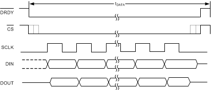
ADS131A02 ADS131A04 DataRetrieve_SynchronousS_sbas590.gifFigure 66. Data Retrieval in Synchronous Slave Mode