ZHCSJF0 February   2019 ADC3244E

PRODUCTION DATA.  

  1. 特性
  2. 应用
  3. 说明
    1.     Device Images
      1.      fS = 125MSPS、fIN = 10MHz 时的性能
  4. 修订历史记录
  5. Device Comparison Table
  6. Pin Configuration and Functions
    1.     Pin Functions
  7. Specifications
    1. 7.1  Absolute Maximum Ratings
    2. 7.2  ESD Ratings
    3. 7.3  Recommended Operating Conditions
    4. 7.4  Thermal Information
    5. 7.5  Electrical Characteristics: General
    6. 7.6  Electrical Characteristics: AC Performance
    7. 7.7  Digital Characteristics
    8. 7.8  Timing Requirements: General
    9. 7.9  Timing Requirements: LVDS Output
    10. 7.10 Typical Characteristics
    11. 7.11 Typical Characteristics: Contour
  8. Parameter Measurement Information
    1. 8.1 Timing Diagrams
  9. Detailed Description
    1. 9.1 Overview
    2. 9.2 Functional Block Diagram
    3. 9.3 Feature Description
      1. 9.3.1 Analog Inputs
      2. 9.3.2 Clock Input
        1. 9.3.2.1 SNR and Clock Jitter
      3. 9.3.3 Digital Output Interface
        1. 9.3.3.1 One-Wire Interface: 14x Serialization
        2. 9.3.3.2 Two-Wire Interface: 7x Serialization
    4. 9.4 Device Functional Modes
      1. 9.4.1 Input Clock Divider
      2. 9.4.2 Chopper Functionality
      3. 9.4.3 Power-Down Control
        1. 9.4.3.1 Improving Wake-Up Time From Global Power-Down
      4. 9.4.4 Internal Dither Algorithm
    5. 9.5 Programming
      1. 9.5.1 Serial Interface
        1. 9.5.1.1 Register Initialization
          1. 9.5.1.1.1 Serial Register Write
          2. 9.5.1.1.2 Serial Register Readout
      2. 9.5.2 Register Initialization
    6. 9.6 Register Maps
      1. 9.6.1 Summary of Special Mode Registers
      2. 9.6.2 Serial Register Description
        1. 9.6.2.1  Register 01h
          1. Table 10. Register 01h Description
        2. 9.6.2.2  Register 03h
          1. Table 11. Register 03h Description
        3. 9.6.2.3  Register 04h
          1. Table 12. Register 04h Description
        4. 9.6.2.4  Register 05h
          1. Table 13. Register 05h Description
        5. 9.6.2.5  Register 06h
          1. Table 14. Register 06h Description
        6. 9.6.2.6  Register 07h
          1. Table 15. Register 07h Description
        7. 9.6.2.7  Register 09h
          1. Table 16. Register 09h Description
        8. 9.6.2.8  Register 0Ah
          1. Table 17. Register 0Ah Description
        9. 9.6.2.9  Register 0Bh
          1. Table 18. Register 0Bh Description
        10. 9.6.2.10 Register 0Eh
          1. Table 19. Register 0Eh Description
        11. 9.6.2.11 Register 0Fh
          1. Table 20. Register 0Fh Description
        12. 9.6.2.12 Register 13h (address = 13h)
          1. Table 21. Register 13h Field Descriptions
        13. 9.6.2.13 Register 15h
          1. Table 23. Register 15h Description
        14. 9.6.2.14 Register 25h
          1. Table 24. Register 25h Description
        15. 9.6.2.15 Register 27h
          1. Table 26. Register 27h Description
        16. 9.6.2.16 Register 41Dh
          1. Table 27. Register 41Dh Description
        17. 9.6.2.17 Register 422h
          1. Table 28. Register 422h Description
        18. 9.6.2.18 Register 434h
          1. Table 29. Register 434h Description
        19. 9.6.2.19 Register 439h
          1. Table 30. Register 439h Description
        20. 9.6.2.20 Register 51Dh
          1. Table 31. Register 51Dh Description
        21. 9.6.2.21 Register 522h
          1. Table 32. Register 522h Description
        22. 9.6.2.22 Register 534h
          1. Table 33. Register 534h Description
        23. 9.6.2.23 Register 539h
          1. Table 34. Register 539h Description
        24. 9.6.2.24 Register 608h
          1. Table 35. Register 608h Description
        25. 9.6.2.25 Register 70Ah
          1. Table 36. Register 70Ah Description
  10. 10Applications and Implementation
    1. 10.1 Application Information
    2. 10.2 Typical Applications
      1. 10.2.1 Driving Circuit Design: Low Input Frequencies
        1. 10.2.1.1 Design Requirements
        2. 10.2.1.2 Detailed Design Procedure
        3. 10.2.1.3 Application Curve
      2. 10.2.2 Driving Circuit Design: Input Frequencies Between 100 MHz to 230 MHz
        1. 10.2.2.1 Design Requirements
        2. 10.2.2.2 Detailed Design Procedure
        3. 10.2.2.3 Application Curve
      3. 10.2.3 Driving Circuit Design: Input Frequencies Greater than 230 MHz
        1. 10.2.3.1 Design Requirements
        2. 10.2.3.2 Detailed Design Procedure
        3. 10.2.3.3 Application Curve
  11. 11Power Supply Recommendations
  12. 12Layout
    1. 12.1 Layout Guidelines
    2. 12.2 Layout Example
  13. 13器件和文档支持
    1. 13.1 接收文档更新通知
    2. 13.2 社区资源
    3. 13.3 商标
    4. 13.4 静电放电警告
    5. 13.5 术语表
  14. 14机械、封装和可订购信息

封装选项

机械数据 (封装 | 引脚)
散热焊盘机械数据 (封装 | 引脚)
订购信息

Clock Input

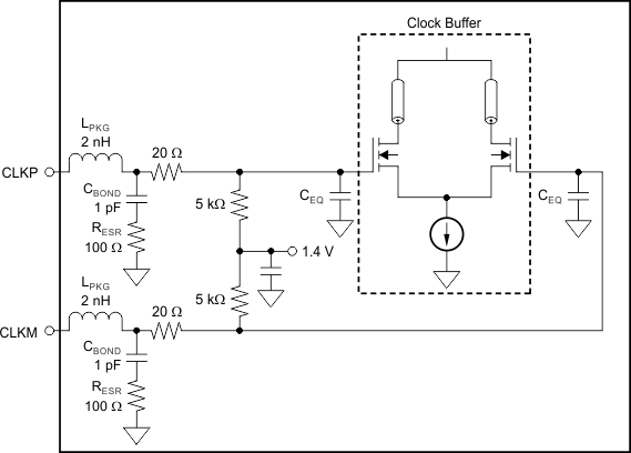
The device clock inputs can be driven differentially (sine, LVPECL, or LVDS) or single-ended (LVCMOS), with little or no difference in performance between them. The common-mode voltage of the clock inputs is set to
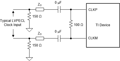
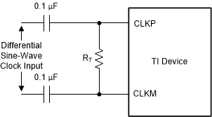
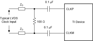
0.95 V using internal 5-kΩ resistors. The self-bias clock inputs of the ADC3244E are driven by the transformer-coupled, sine-wave clock source or by the ac-coupled, LVPECL and LVDS clock sources, as shown in Figure 43, Figure 44, and Figure 45. See Figure 46 for details regarding the internal clock buffer.
ADC3244E ai_dif_sinewave_clk_bas550.gif
NOTE: RT = termination resistor, if necessary.
Figure 43. Differential Sine-Wave Clock Driving Circuit
ADC3244E ai_lvds_clk_drv_bas550.gifFigure 44. LVDS Clock Driving Circuit
ADC3244E ai_lvpecl_clk_drv_bas550.gifFigure 45. LVPECL Clock Driving Circuit
ADC3244E ai_intclk_buffer_las900.gif
NOTE: CEQ is 1 pF to 3 pF and is the equivalent input capacitance of the clock buffer.
Figure 46. Internal Clock Buffer

A single-ended CMOS clock can be ac-coupled to the CLKP input, with CLKM connected to ground with a 0.1-μF capacitor, as shown in Figure 47. However, for best performance the clock inputs must be driven differentially, thereby reducing susceptibility to common-mode noise. For high input frequency sampling, TI recommends using a clock source with very low jitter. Band-pass filtering of the clock source can help reduce the effects of jitter. There is no change in performance with a non-50% duty cycle clock input.
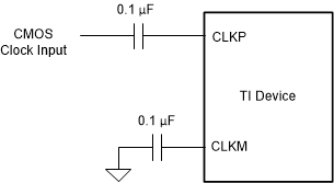
ADC3244E ai_drv_cir_1end_las900.gifFigure 47. Single-Ended Clock Driving Circuit