ZHCSBB4B July 2013 – June 2017 TPS61197
PRODUCTION DATA.
- 1 特性
- 2 应用范围
- 3 说明
- 4 修订历史记录
- 5 Pin Configuration and Functions
- 6 Specifications
-
7 Detailed Description
- 7.1 Overview
- 7.2 Functional Block Diagram
- 7.3 Feature Description
- 7.4
Device Functional Modes
- 7.4.1
Protections
- 7.4.1.1 Switch Current Limit Protection Using the ISNS Pin
- 7.4.1.2 LED Open Protection
- 7.4.1.3 Schottky Diode Open Protection
- 7.4.1.4 Schottky Diode Short Protection
- 7.4.1.5 IFB Overvoltage Protection
- 7.4.1.6 Output Overvoltage Protection Using the OVP Pin
- 7.4.1.7 IFB Short-to-Ground Protection
- 7.4.1.8 Thermal Shutdown
- 7.4.1
Protections
- 8 Application and Implementation
- 9 Power Supply Recommendations
- 10Layout
- 11器件和文档支持
- 12机械、封装和可订购信息
7.3.4 Enable and Undervoltage Lockout
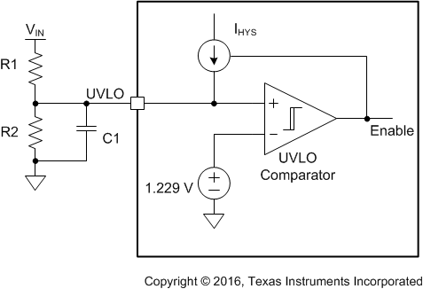
The TPS61197 is enabled with soft start-up when the EN pin voltage is higher than 1.6 V. A voltage of less than 0.75 V disables the TPS61197. An undervoltage lockout (UVLO) protection feature is provided in the TPS61197. When the voltage at the VIN pin is less than 6.5 V, the TPS61197 is powered off. The TPS61197 resumes the operation once the voltage at the VIN pin recovers above the hysteresis (VVIN_HYS ) more than the UVLO falling threshold of input voltage. If a higher UVLO voltage is required, use the UVLO pin as shown in Figure 15 to adjust the input UVLO threshold by using an external resistor divider. Once the voltage at the UVLO pin exceeds the 1.229-V threshold, the TPS61197 is powered on and a hysteresis current source of 3.9 µA is added. When the voltage at the UVLO pin drops lower than 1.229 V, the current source is removed and the TPS61197 is powered off. The resistors of R1, R2 can be calculated by Equation 2 from required turnon voltage (VSTART) and turn-off voltage (VSTOP). To avoid noise coupling, the resistor divider R1 and R2 must be close to the UVLO pin. Placing a filter capacitor of more than 10nF as shown in Figure 15 can eliminate the impact of the switching ripple of the input voltage and improve the noise immunity.
If the UVLO function is not used, pull up the UVLO pin to the VDD pin.
 Figure 15. UVLO Circuit

where
- IHYS is 3.9 µA sourcing current from the UVLO pin

When the UVLO condition happens, the FAULT pin outputs high impedance. As long as the UVLO condition is removed, the FAULT pin outputs low impedance.