ZHCSBB4B July   2013  – June 2017 TPS61197

PRODUCTION DATA.  

  1. 特性
  2. 应用范围
  3. 说明
    1.     Device Images
      1.      简化原理图
  4. 修订历史记录
  5. Pin Configuration and Functions
    1.     Pin Functions
  6. Specifications
    1. 6.1 Absolute Maximum Ratings
    2. 6.2 ESD Ratings
    3. 6.3 Recommended Operating Conditions
    4. 6.4 Thermal Information
    5. 6.5 Electrical Characteristics
    6. 6.6 Switching Characteristics
    7. 6.7 Typical Characteristics
  7. Detailed Description
    1. 7.1 Overview
    2. 7.2 Functional Block Diagram
    3. 7.3 Feature Description
      1. 7.3.1 Supply Voltage
      2. 7.3.2 Boost Controller
      3. 7.3.3 Switching Frequency
      4. 7.3.4 Enable and Undervoltage Lockout
      5. 7.3.5 Power-Up Sequencing and Soft Start-up
      6. 7.3.6 Current Regulation
      7. 7.3.7 PWM Dimming
      8. 7.3.8 Indication for Fault Conditions
    4. 7.4 Device Functional Modes
      1. 7.4.1 Protections
        1. 7.4.1.1 Switch Current Limit Protection Using the ISNS Pin
        2. 7.4.1.2 LED Open Protection
        3. 7.4.1.3 Schottky Diode Open Protection
        4. 7.4.1.4 Schottky Diode Short Protection
        5. 7.4.1.5 IFB Overvoltage Protection
        6. 7.4.1.6 Output Overvoltage Protection Using the OVP Pin
        7. 7.4.1.7 IFB Short-to-Ground Protection
        8. 7.4.1.8 Thermal Shutdown
  8. Application and Implementation
    1. 8.1 Application Information
    2. 8.2 Typical Applications
      1. 8.2.1 Simple Boost Converter
        1. 8.2.1.1 Design Requirements
        2. 8.2.1.2 Detailed Design Procedure
          1. 8.2.1.2.1 Inductor Selection
          2. 8.2.1.2.2 Output Capacitor
          3. 8.2.1.2.3 Schottky Diode
          4. 8.2.1.2.4 Switch MOSFET and Gate Driver Resistor
          5. 8.2.1.2.5 Current Sense and Current Sense Filtering
          6. 8.2.1.2.6 Loop Consideration
        3. 8.2.1.3 Application Curves
      2. 8.2.2 PWM Dimming Controlled by Boost Converter
      3. 8.2.3 High Boost Ratio Application
  9. Power Supply Recommendations
  10. 10Layout
    1. 10.1 Layout Guidelines
    2. 10.2 Layout Example
  11. 11器件和文档支持
    1. 11.1 接收文档更新通知
    2. 11.2 社区资源
    3. 11.3 商标
    4. 11.4 静电放电警告
    5. 11.5 Glossary
  12. 12机械、封装和可订购信息

封装选项

机械数据 (封装 | 引脚)
散热焊盘机械数据 (封装 | 引脚)
订购信息

Typical Characteristics

Table 1. Table Of Graphs

See Figure 18
TITLE TEST CONDITIONS FIGURE
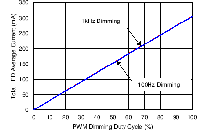
Dimming Linearity 24 LEDs (VOUT = 80 V), VIN = 24 V Figure 1
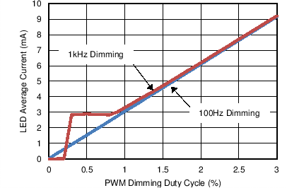
Dimming Linearity at Small Dimming Duty Cycle 24 LEDs (VOUT = 80 V), VIN = 24 V Figure 2
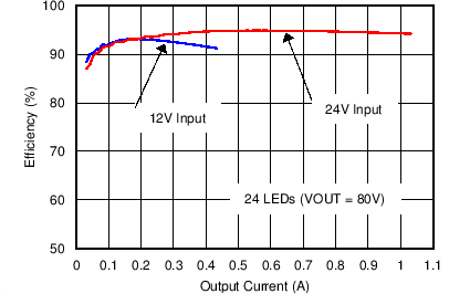
DC Load Efficiency fSW = 130 kHz Figure 3
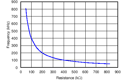
Switching Frequency Setting VIN = 24 V Figure 4
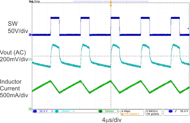
Boost Switching Waveform VIN = 24 V, VOUT = 80 V, IOUT = 300 mA Figure 5
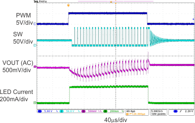
Dimming Waveform (2% Dimming) VIN = 24 V, VOUT = 80 V, IOUT = 300 mA, 100-Hz dimming frequency Figure 6
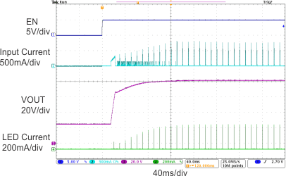
Startup Waveform (1% Dimming) 100-Hz dimming frequency, 1% dimming duty cycle Figure 7
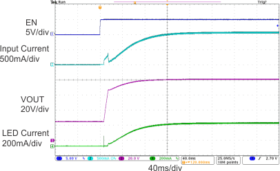
Startup Waveform (100% Dimming) 100-Hz dimming frequency, 100% dimming duty cycle Figure 8
Shutdown Waveform (1% Dimming) 100-Hz dimming frequency, 1% dimming duty cycle Figure 9
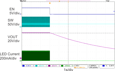
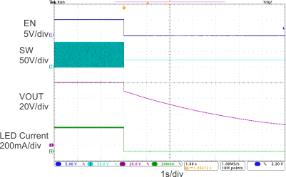
Shutdown Waveform (100% Dimming) 100-Hz dimming frequenc, 100% dimming duty cycle Figure 10
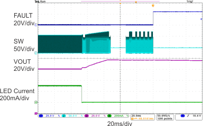
LED Open Protection (1% Dimming) 100-Hz dimming frequenc, 1% dimming duty cycle Figure 11
LED Open Protection (100% Dimming) 100-Hz dimming frequenc, 100% Dimming Duty Cycle Figure 12
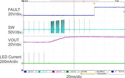
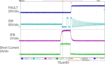
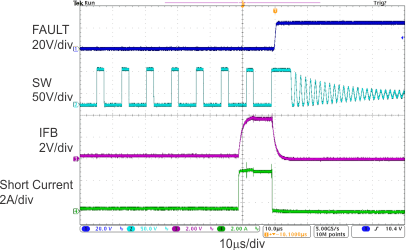
LED String Short Protection (1% Dimming) 100-Hz dimming frequency, 1% dimming duty cycle Figure 13
LED String Short Protection (100% Dimming) 100-Hz dimming frequency, 1% dimming duty cycle Figure 14
TPS61197 C003_SLVSC25.png
Figure 1. Dimming Linearity
TPS61197 C005_SLVSC25.png
Figure 3. DC Load Efficiency
TPS61197 C004_SLVSC25.png
Figure 2. Dimming Linearity at Low Dimming Duty Cycle
TPS61197 C006_SLVSC25.png
Figure 4. Switching Frequency Setting
TPS61197 S1_lvsc25.gif
Figure 5. Boost Switching Waveform
TPS61197 S3_lvsc25.gif
Figure 7. Start-up Waveform (1% Dimming)
TPS61197 S5_lvsc25.gif
Figure 9. Shutdown Waveform (1% Dimming)
TPS61197 S7_lvsc25.gif
Figure 11. LED Open Protection (1% Dimming)
TPS61197 S9_lvsc25.gif
Figure 13. LED String Short Protection (1% Dimming)
TPS61197 S2_lvsc25.gif
Figure 6. Dimming Waveform (1% Dimming)
TPS61197 S4_lvsc25.gif
Figure 8. Start-up Waveform (100% Dimming)
TPS61197 S6_lvsc25.gif
Figure 10. Shutdown Waveform (100% Dimming)
TPS61197 S8_lvsc25.gif
Figure 12. LED Open Protection (100% Dimming)
TPS61197 S10_lvsc25.gif
Figure 14. LED String Short Protection (100% Dimming)