ZHCSFH8D August   2016  – January 2018 TPS25741 , TPS25741A

UNLESS OTHERWISE NOTED, this document contains PRODUCTION DATA.  

  1. 特性
  2. 应用
  3. 说明
    1.     Device Images
      1.      DFP 主机端口中的简化实施方案
  4. 修订历史记录
  5. Device Comparison Table
  6. Pin Configuration and Functions
    1.     Pin Functions
  7. Specifications
    1. 7.1 Absolute Maximum Ratings
    2. 7.2 ESD Ratings
    3. 7.3 Recommended Operating Conditions
    4. 7.4 Thermal Information
    5. 7.5 Electrical Characteristics
    6. 7.6 Timing Requirements
    7. 7.7 Switching Characteristics
    8. 7.8 Typical Characteristics
  8. Detailed Description
    1. 8.1 Overview
      1. 8.1.1 VBUS Capacitance
      2. 8.1.2 USB Data Communications
    2. 8.2 Functional Block Diagram
    3. 8.3 Feature Description
      1. 8.3.1  USB Type-C CC Logic (CC1, CC2)
      2. 8.3.2  9.3.2 VCONN Supply (VCONN, CC1, CC2)
      3. 8.3.3  USB Power Delivery BMC Transmission (CC1, CC2, VTX)
      4. 8.3.4  USB Power Delivery BMC Reception (CC1, CC2)
      5. 8.3.5  Discharging (DSCG, VPWR)
        1. 8.3.5.1 Discharging after a Fault (VPWR)
      6. 8.3.6  Configuring Voltage Capabilities (HIPWR, EN9V, EN12V)
      7. 8.3.7  Configuring Power Capabilities (PSEL, PCTRL, HIPWR)
      8. 8.3.8  Gate Drivers
        1. 8.3.8.1 GDNG, GDNS
        2. 8.3.8.2 G5V
        3. 8.3.8.3 GDPG
      9. 8.3.9  Fault Monitoring and Protection
        1. 8.3.9.1 Over/Under Voltage (VBUS)
        2. 8.3.9.2 Over-Current Protection (ISNS, VBUS)
        3. 8.3.9.3 System Fault Input (GD, VPWR)
      10. 8.3.10 Voltage Control (CTL1, CTL2)
      11. 8.3.11 Sink Attachment Indicator (UFP, DVDD)
      12. 8.3.12 Accessory Attachment Indicator (AUDIO, DEBUG)
      13. 8.3.13 Plug Polarity Indication (POL)
      14. 8.3.14 Power Supplies (VAUX, VDD, VPWR, DVDD)
      15. 8.3.15 Grounds (AGND, GND)
      16. 8.3.16 Output Power Supply (DVDD)
    4. 8.4 Device Functional Modes
      1. 8.4.1 Sleep Mode
      2. 8.4.2 Checking VBUS at Start Up
  9. Application and Implementation
    1. 9.1 Application Information
      1. 9.1.1 System-Level ESD Protection
      2. 9.1.2 Use of GD Internal Clamp
      3. 9.1.3 Resistor Divider on GD for Programmable Start Up
      4. 9.1.4 Selection of the CTL1 and CTL2 Resistors (RFBL1 and RFBL2)
      5. 9.1.5 Voltage Transition Requirements
      6. 9.1.6 VBUS Slew Control using GDNG CSLEW
      7. 9.1.7 Tuning OCP Using RF and CF
    2. 9.2 Typical Applications
      1. 9.2.1 A/C Multiplexing Power Source
        1. 9.2.1.1 Design Requirements
        2. 9.2.1.2 Detailed Design Procedure
          1. 9.2.1.2.1 Power Pin Bypass Capacitors
          2. 9.2.1.2.2 Non-Configurable Components
          3. 9.2.1.2.3 Configurable Components
        3. 9.2.1.3 Application Curves
      2. 9.2.2 D/C Power Source
        1. 9.2.2.1 Design Requirements
        2. 9.2.2.2 Detailed Design Procedure
          1. 9.2.2.2.1 Power Pin Bypass Capacitors
          2. 9.2.2.2.2 Non-Configurable Components
          3. 9.2.2.2.3 Configurable Components
        3. 9.2.2.3 Application Curves
    3. 9.3 System Examples
      1. 9.3.1 A/C Power Source (Wall Adapter)
      2. 9.3.2 Dual-Port Power Managed A/C Power Source (Wall Adapter)
  10. 10Power Supply Recommendations
    1. 10.1 VDD
    2. 10.2 VCONN
    3. 10.3 VPWR
  11. 11Layout
    1. 11.1 Layout Guidelines
      1. 11.1.1 Port Current Kelvin Sensing
      2. 11.1.2 Power Pin Bypass Capacitors
      3. 11.1.3 Supporting Components
    2. 11.2 Layout Example
  12. 12器件和文档支持
    1. 12.1 Documentation Support
    2. 12.2 相关链接
    3. 12.3 Receiving Notification of Documentation Updates
    4. 12.4 Community Resources
    5. 12.5 商标
    6. 12.6 静电放电警告
    7. 12.7 Glossary
  13. 13机械、封装和可订购信息

封装选项

机械数据 (封装 | 引脚)
散热焊盘机械数据 (封装 | 引脚)
订购信息

Power Supplies (VAUX, VDD, VPWR, DVDD)

The VAUX pin is the output of a linear regulator and the input supply for internal power management circuitry. The VAUX regulator draws power from VDD after establishing a USB Power Delivery contract unless it is not available in which case it draws from VPWR. Changes in supply voltages will result in seamless switching between supplies.

If there is a load on the DVDD pin, that current will be drawn from the VPWR pin unless the TPS25741/TPS25741A has stabilized into a USB Power Delivery contract or VPWR is below its UVLO.

The TPS25741/TPS25741A cannot function properly until VPWR is above its UVLO. However, for improved system efficiency when UFP is high-z, VPWR can be low (the high voltage power supply can be disabled) if VDD is above its UVLO.

Connect a 0.1-µF ceramic capacitor from VAUX to GND. Do not connect any external load that draws more than IVAUXEXT. Locate the bypass capacitor close to the pin and provide a low impedance ground connection from the capacitor to the ground plane.

VDD should either be grounded or be fed by a low impedance path and have input bypass capacitance. Locate the bypass capacitors close to the VDD and VPWR pins and provide a low impedance ground connection from the capacitor to the ground plane.
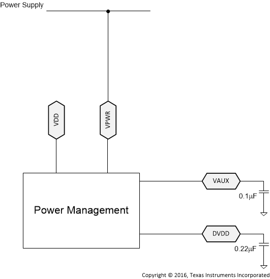
TPS25741 TPS25741A Pwr_mgmt_slvsdj5.gifFigure 40. Power Management