ZHCSFH8D August 2016 – January 2018 TPS25741 , TPS25741A
UNLESS OTHERWISE NOTED, this document contains PRODUCTION DATA.
- 1 特性
- 2 应用
- 3 说明
- 4 修订历史记录
- 5 Device Comparison Table
- 6 Pin Configuration and Functions
- 7 Specifications
-
8 Detailed Description
- 8.1 Overview
- 8.2 Functional Block Diagram
- 8.3
Feature Description
- 8.3.1 USB Type-C CC Logic (CC1, CC2)
- 8.3.2 9.3.2 VCONN Supply (VCONN, CC1, CC2)
- 8.3.3 USB Power Delivery BMC Transmission (CC1, CC2, VTX)
- 8.3.4 USB Power Delivery BMC Reception (CC1, CC2)
- 8.3.5 Discharging (DSCG, VPWR)
- 8.3.6 Configuring Voltage Capabilities (HIPWR, EN9V, EN12V)
- 8.3.7 Configuring Power Capabilities (PSEL, PCTRL, HIPWR)
- 8.3.8 Gate Drivers
- 8.3.9 Fault Monitoring and Protection
- 8.3.10 Voltage Control (CTL1, CTL2)
- 8.3.11 Sink Attachment Indicator (UFP, DVDD)
- 8.3.12 Accessory Attachment Indicator (AUDIO, DEBUG)
- 8.3.13 Plug Polarity Indication (POL)
- 8.3.14 Power Supplies (VAUX, VDD, VPWR, DVDD)
- 8.3.15 Grounds (AGND, GND)
- 8.3.16 Output Power Supply (DVDD)
- 8.4 Device Functional Modes
- 9 Application and Implementation
- 10Power Supply Recommendations
- 11Layout
- 12器件和文档支持
- 13机械、封装和可订购信息
8.3.5 Discharging (DSCG, VPWR)
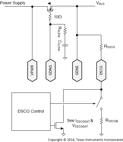
The DSCG pin allows for two different pull-downs that are used to apply different discharging strengths. In addition, a load may be applied to the VPWR pin to discharge the power supply.
If too much power is dissipated by the device (that is, the TJ1 temperature is exceeded) an OTSD occurs that disables the discharge FET; therefore, an external resistor is recommended in series with the DSCG pin to absorb most of the dissipated power. The external resistor RDSCG should be chosen such that the current sunk by the DSCG pin does not exceed IDSCGT.
The VPWR pin should always be connected to the supply side (as opposed to the connector side) of the power-path switch (Figure 31 shows one example). This pin is monitored before enabling the GDNG gate driver to apply the voltage to the VBUS pin of the connector.
From sink attachment, and while the device has not finalized a USB Power Delivery contract, the device applies RDSCGB.
Also from sink attachment, and while the device has not finalized a USB Power Delivery contract, the device draws ISUPP through the VPWR pin even if VDD is above its UVLO. This helps to discharge the power supply source bulk capacitance.
 Figure 31. Discharge Schematic
The discharge procedure used in the TPS25741 or TPS25741A is intended to allow the DSCG pin to help pull the power supply down from high voltage, and then also pull VBUS at the connector down to the required level quickly (refer to USB Power Delivery in Documentation Support).