ZHCSFH8D August 2016 – January 2018 TPS25741 , TPS25741A
UNLESS OTHERWISE NOTED, this document contains PRODUCTION DATA.
- 1 特性
- 2 应用
- 3 说明
- 4 修订历史记录
- 5 Device Comparison Table
- 6 Pin Configuration and Functions
- 7 Specifications
-
8 Detailed Description
- 8.1 Overview
- 8.2 Functional Block Diagram
- 8.3
Feature Description
- 8.3.1 USB Type-C CC Logic (CC1, CC2)
- 8.3.2 9.3.2 VCONN Supply (VCONN, CC1, CC2)
- 8.3.3 USB Power Delivery BMC Transmission (CC1, CC2, VTX)
- 8.3.4 USB Power Delivery BMC Reception (CC1, CC2)
- 8.3.5 Discharging (DSCG, VPWR)
- 8.3.6 Configuring Voltage Capabilities (HIPWR, EN9V, EN12V)
- 8.3.7 Configuring Power Capabilities (PSEL, PCTRL, HIPWR)
- 8.3.8 Gate Drivers
- 8.3.9 Fault Monitoring and Protection
- 8.3.10 Voltage Control (CTL1, CTL2)
- 8.3.11 Sink Attachment Indicator (UFP, DVDD)
- 8.3.12 Accessory Attachment Indicator (AUDIO, DEBUG)
- 8.3.13 Plug Polarity Indication (POL)
- 8.3.14 Power Supplies (VAUX, VDD, VPWR, DVDD)
- 8.3.15 Grounds (AGND, GND)
- 8.3.16 Output Power Supply (DVDD)
- 8.4 Device Functional Modes
- 9 Application and Implementation
- 10Power Supply Recommendations
- 11Layout
- 12器件和文档支持
- 13机械、封装和可订购信息
8.3.5.1 Discharging after a Fault (VPWR)
There are two types of faults that cause the TPS25741 or TPS25741A to begin a full discharge of VBUS: Slow-shutdown faults and fast-shutdown faults. When a slow-shutdown fault occurs, the device does not disable GDNG until after VBUS is measured below VSOVP (for 5 V contract). When a fast-shutdown fault occurs, the device disables GDNG immediately and then discharges the connector side of the power-path. In both cases, the bleed discharge is applied to the DSCG pin and ISUPP is drawn from the VPWR pin.
Slow-shutdown faults that do not include transmitting a hard reset:
- Receiving a Hard Reset signal (25 ms < tShutdownDelay< 35 ms)
- Cable is unplugged (tShutdownDelay< 20 µs)
Slow-shutdown faults that include transmitting hard reset (25 ms < tShutdownDelay< 35 ms)
- TJ exceeds TJ1 (an overtemperature event)
- Low voltage alarm occurring outside of a voltage transition
- High voltage alarm occurring outside of a voltage transition (but not high enough to cause OVP)
- Receiving an unexpected message during a voltage transition
- Failure of power supply to transition voltages within required time of 600 ms (tPSTransition [refer to USB Power Delivery in Documentation Support]).
- A Soft Reset USB Power Delivery message is not acknowledged or Accepted (as required per USB Power Delivery in Documentation Support).
- A Request USB Power Delivery message is not received in the required time (as required per USB Power Delivery in Documentation Support).
- Failure to discharge down to 0.725 V after a fault of any kind.
Fast-shutdown faults (hard reset always sent):
- Fast OVP event occurring at any time.
- OCP event occurring at any time starting from the transmission of the first USB Power Delivery message.
- VBUS falling below VBUS_FTH is treated as an OVP event.
- GD falling edge
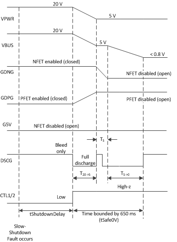
The DSCG pin is used to discharge the supply line after a slow-shutdown fault occurs. Figure 32 illustrates the signals involved. Depending on the specific slow-shutdown fault the time tShutdownDelay in Figure 32 is different as indicated in the list above. If the slow-shutdown fault triggers a hard reset, it is sent at the beginning of the tShutdownDelay period. However, the device behavior after the time tShutdownDelay is the same for all slow-shutdown faults. After the tShutdownDelay period, the device sets CTL1 and CTL2 to select 5 V from the power supply and puts the DSCG pin into its ON state (Full Discharge). This discharging continues until the voltage on the VBUS pin reaches VSOPV (for 5 V contract). The device then disables GDNG and again puts the DSCG pin into its ON state. This discharging state lasts until the voltage on VBUS reaches 0.725 V (nominal). If the discharge does not complete within 650 ms, then the device sends a Hard Reset signal and the process repeats. In Figure 32, the times labeled as T20->5 and T5->0 can vary, they depend on the size of the capacitance to be discharged and the size of the external resistor between the DSCG pin and VBUS. The time labeled as TS is a function of how quickly the NFET opens.
 Figure 32. Illustration of Slow-Shutdown VBUS Discharge
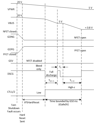
Figure 33 illustrates a similar discharge procedure for fast-shutdown faults. The main difference from Figure 32 is that the NFET is opened immediately. It is assumed for the purposes of this illustration that the power supply output capacitance (that is, CSOURCE in the reference schematics shown in Figure 20 and Figure 21) is not discharged by the power supply itself, but the VPWR pin is bleeding current from that capacitance. The VPWR pin then draws ISUPP after GDNG disables the external NFET. So, as shown in the figure, the VPWR voltage discharges slowly, while the VBUS pin is discharged quickly once the full discharge is enabled. If the voltage on the VPWR pin takes longer than T20->5 + T5->0 + 0.765s to discharge below VFOVP, then it causes an OVP event and the process repeats.
 Figure 33. Illustration of Fast-Shutdown Discharge
If the discharge does not complete successfully it is treated as a slow-shutdown fault, and the TPS25741 or TPS25741A repeats the discharge procedure until it does complete successfully. Once the discharge completes successfully as described above (that is, VBUS on connector is below 0.725 V), the device waits for 0.765 s (nominal) before trying to source VBUS again.