ZHCSHR3B June 2017 – August 2020 LMR23615
PRODUCTION DATA
- 1 特性
- 2 应用
- 3 说明
- 4 Revision History
- 5 Pin Configuration and Functions
- 6 Specifications
-
7 Detailed Description
- 7.1 Overview
- 7.2 Functional Block Diagram
- 7.3
Feature Description
- 7.3.1 Fixed-Frequency, Peak-Current-Mode Control
- 7.3.2 Adjustable Frequency
- 7.3.3 Adjustable Output Voltage
- 7.3.4 Enable/Sync
- 7.3.5 VCC, UVLO
- 7.3.6 Minimum ON-Time, Minimum-OFF Time, and Frequency Foldback at Dropout Conditions
- 7.3.7 Internal Compensation and CFF
- 7.3.8 Bootstrap Voltage (BOOT)
- 7.3.9 Overcurrent and Short-Circuit Protection
- 7.3.10 Thermal Shutdown
- 7.4 Device Functional Modes
-
8 Application and Implementation
- 8.1 Application Information
- 8.2
Typical Applications
- 8.2.1 Design Requirements
- 8.2.2
Detailed Design Procedure
- 8.2.2.1 Custom Design With WEBENCH® Tools
- 8.2.2.2 Output Voltage Setpoint
- 8.2.2.3 Switching Frequency
- 8.2.2.4 Inductor Selection
- 8.2.2.5 Output Capacitor Selection
- 8.2.2.6 Feedforward Capacitor
- 8.2.2.7 Input Capacitor Selection
- 8.2.2.8 Bootstrap Capacitor Selection
- 8.2.2.9 VCC Capacitor Selection
- 8.2.2.10 Undervoltage Lockout Setpoint
- 8.2.3 Application Curves
- 9 Power Supply Recommendations
- 10Layout
- 11Device and Documentation Support
- 12Mechanical, Packaging, and Orderable Information
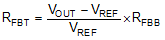
7.3.3 Adjustable Output Voltage
A precision 1-V reference voltage is used to maintain a tightly regulated output voltage over the entire operating temperature range. The output voltage is set by a resistor divider from output voltage to the FB pin. TI recommends using 1% tolerance resistors with a low temperature coefficient for the FB divider. Select the low-side resistor RFBB for the desired divider current and use Equation 2 to calculate high-side RFBT. RFBT in the range from 10 kΩ to 100 kΩ is recommended for most applications. A lower RFBT value can be used if static loading is desired to reduce VOUT offset in PFM operation. Lower RFBT reduces efficiency at very light load. Less static current goes through a larger RFBT and might be more desirable when light load efficiency is critical. However, RFBT larger than 1 MΩ is not recommended because it makes the feedback path more susceptible to noise. Larger RFBT value requires more carefully designed feedback path on the PCB. The tolerance and temperature variation of the resistor dividers affect the output voltage regulation.
 Figure 7-3 Output Voltage Setting