ZHCSHR3B June 2017 – August 2020 LMR23615
PRODUCTION DATA
- 1 特性
- 2 应用
- 3 说明
- 4 Revision History
- 5 Pin Configuration and Functions
- 6 Specifications
-
7 Detailed Description
- 7.1 Overview
- 7.2 Functional Block Diagram
- 7.3
Feature Description
- 7.3.1 Fixed-Frequency, Peak-Current-Mode Control
- 7.3.2 Adjustable Frequency
- 7.3.3 Adjustable Output Voltage
- 7.3.4 Enable/Sync
- 7.3.5 VCC, UVLO
- 7.3.6 Minimum ON-Time, Minimum-OFF Time, and Frequency Foldback at Dropout Conditions
- 7.3.7 Internal Compensation and CFF
- 7.3.8 Bootstrap Voltage (BOOT)
- 7.3.9 Overcurrent and Short-Circuit Protection
- 7.3.10 Thermal Shutdown
- 7.4 Device Functional Modes
-
8 Application and Implementation
- 8.1 Application Information
- 8.2
Typical Applications
- 8.2.1 Design Requirements
- 8.2.2
Detailed Design Procedure
- 8.2.2.1 Custom Design With WEBENCH® Tools
- 8.2.2.2 Output Voltage Setpoint
- 8.2.2.3 Switching Frequency
- 8.2.2.4 Inductor Selection
- 8.2.2.5 Output Capacitor Selection
- 8.2.2.6 Feedforward Capacitor
- 8.2.2.7 Input Capacitor Selection
- 8.2.2.8 Bootstrap Capacitor Selection
- 8.2.2.9 VCC Capacitor Selection
- 8.2.2.10 Undervoltage Lockout Setpoint
- 8.2.3 Application Curves
- 9 Power Supply Recommendations
- 10Layout
- 11Device and Documentation Support
- 12Mechanical, Packaging, and Orderable Information
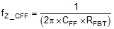
7.3.7 Internal Compensation and CFF
The LMR23615 is internally compensated as shown in Section 7.2. The internal compensation is designed such that the loop response is stable over the entire operating frequency and output voltage range. Depending on the output voltage, the compensation loop phase margin can be low with all ceramic capacitors. An external feedforward capacitor CFF is recommended to be placed in parallel with the top resistor divider RFBT for optimum transient performance.
 Figure 7-9 Feedforward Capacitor for Loop Compensation
The feedforward capacitor CFF in parallel with RFBT places an additional zero before the crossover frequency of the control loop to boost phase margin. The zero frequency can be found by
An additional pole is also introduced with CFF at the frequency of
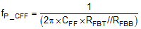
The zero fZ_CFF adds phase boost at the crossover frequency and improves transient response. The pole fP-CFF helps maintaining proper gain margin at frequency beyond the crossover. Table 8-1 lists the combination of COUT, CFF and RFBT for typical applications, designs with similar COUT but RFBT other than recommended value, adjust CFF such that (CFF × RFBT) is unchanged and adjust RFBB such that (RFBT / RFBB) is unchanged.
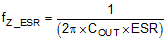
Designs with different combinations of output capacitors need different CFF. Different types of capacitors have different equivalent series resistance (ESR). Ceramic capacitors have the smallest ESR and need the most CFF. Electrolytic capacitors have much larger ESR than ceramic, and the ESR zero frequency location would be low enough to boost the phase up around the crossover frequency. Designs that use mostly electrolytic capacitors at the output may not need any CFF. The location of this ESR zero frequency can be calculated with Equation 9:
The CFF creates a time constant with RFBT that couples in the attenuate output voltage ripple to the FB node. If the CFF value is too large, it can couple too much ripple to the FB and affect VOUT regulation. Therefore, calculate CFF based on output capacitors used in the system. At cold temperatures, the value of CFF might change based on the tolerance of the chosen component. This may reduce its impedance and ease noise coupling on the FB node. To avoid this, more capacitance can be added to the output or the value of CFF can be reduced.