ZHCSHR3B June 2017 – August 2020 LMR23615
PRODUCTION DATA
- 1 特性
- 2 应用
- 3 说明
- 4 Revision History
- 5 Pin Configuration and Functions
- 6 Specifications
-
7 Detailed Description
- 7.1 Overview
- 7.2 Functional Block Diagram
- 7.3
Feature Description
- 7.3.1 Fixed-Frequency, Peak-Current-Mode Control
- 7.3.2 Adjustable Frequency
- 7.3.3 Adjustable Output Voltage
- 7.3.4 Enable/Sync
- 7.3.5 VCC, UVLO
- 7.3.6 Minimum ON-Time, Minimum-OFF Time, and Frequency Foldback at Dropout Conditions
- 7.3.7 Internal Compensation and CFF
- 7.3.8 Bootstrap Voltage (BOOT)
- 7.3.9 Overcurrent and Short-Circuit Protection
- 7.3.10 Thermal Shutdown
- 7.4 Device Functional Modes
-
8 Application and Implementation
- 8.1 Application Information
- 8.2
Typical Applications
- 8.2.1 Design Requirements
- 8.2.2
Detailed Design Procedure
- 8.2.2.1 Custom Design With WEBENCH® Tools
- 8.2.2.2 Output Voltage Setpoint
- 8.2.2.3 Switching Frequency
- 8.2.2.4 Inductor Selection
- 8.2.2.5 Output Capacitor Selection
- 8.2.2.6 Feedforward Capacitor
- 8.2.2.7 Input Capacitor Selection
- 8.2.2.8 Bootstrap Capacitor Selection
- 8.2.2.9 VCC Capacitor Selection
- 8.2.2.10 Undervoltage Lockout Setpoint
- 8.2.3 Application Curves
- 9 Power Supply Recommendations
- 10Layout
- 11Device and Documentation Support
- 12Mechanical, Packaging, and Orderable Information
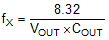
8.2.2.6 Feedforward Capacitor
The LMR23615 device is internally compensated. Depending on the VOUT and frequency fSW, if the output capacitor COUT is dominated by low ESR (ceramic types) capacitors, it could result in low phase margin. To improve the phase boost an external feedforward capacitor CFF can be added in parallel with RFBT. CFF is chosen such that phase margin is boosted at the crossover frequency without CFF. A simple estimation for the crossover frequency (fX) without CFF is shown in Equation 18, assuming COUT has very small ESR, and COUT value is after derating.
Equation 19 for CFF was tested:
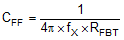
For designs with higher ESR, CFF is not needed when COUT has very high ESR, and CFF calculated from Equation 19 should be reduced with medium ESR. Table 8-1 can be used as a quick starting point.
For the application in this design example, a 18-pF, 50-V, COG capacitor is selected.