ZHCSEY3D April 2016 – October 2019 DS90UB914A-Q1
PRODUCTION DATA.
- 1 特性
- 2 应用
- 3 说明
- 4 修订历史记录
- 5 Device Comparison Table
- 6 Pin Configuration and Functions
-
7 Specifications
- 7.1 Absolute Maximum Ratings
- 7.2 ESD Ratings
- 7.3 Recommended Operating Conditions
- 7.4 Thermal Information
- 7.5 Electrical Characteristics
- 7.6 AC Timing Specifications (SCL, SDA) - I2C-Compatible
- 7.7 Bidirectional Control Bus DC Timing Specifications (SCL, SDA) - I2C-Compatible
- 7.8 Deserializer Switching Characteristics
- 7.9 Typical Characteristics
- 8 Parameter Measurement Information
-
9 Detailed Description
- 9.1 Overview
- 9.2 Functional Block Diagram
- 9.3
Feature Description
- 9.3.1 Serial Frame Format
- 9.3.2 Line Rate Calculations for the DS90UB913A/914A
- 9.3.3 Deserializer Multiplexer Input
- 9.3.4 Error Detection
- 9.3.5 Synchronizing Multiple Cameras
- 9.3.6 General-Purpose I/O (GPIO) Descriptions
- 9.3.7 LVCMOS VDDIO Option
- 9.3.8 EMI Reduction
- 9.3.9 Pixel Clock Edge Select (TRFB / RRFB)
- 9.3.10 Power Down
- 9.4
Device Functional Modes
- 9.4.1 DS90UB913A/914A Operation With External Oscillator as Reference Clock
- 9.4.2 DS90UB913A/914A Operation With Pixel Clock From Imager as Reference Clock
- 9.4.3 MODE Pin on Deserializer
- 9.4.4 Clock-Data Recovery Status Flag (LOCK), Output Enable (OEN) and Output State Select (OSS_SEL)
- 9.4.5 Built-In Self Test
- 9.4.6 BIST Configuration and Status
- 9.4.7 Sample BIST Sequence
- 9.5 Programming
- 9.6 Register Maps
- 10Application and Implementation
- 11Power Supply Recommendations
- 12Layout
- 13器件和文档支持
- 14机械、封装和可订购信息
12.2 Layout Example
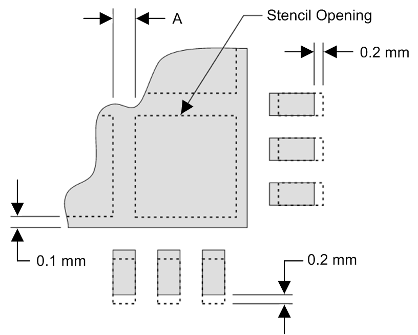
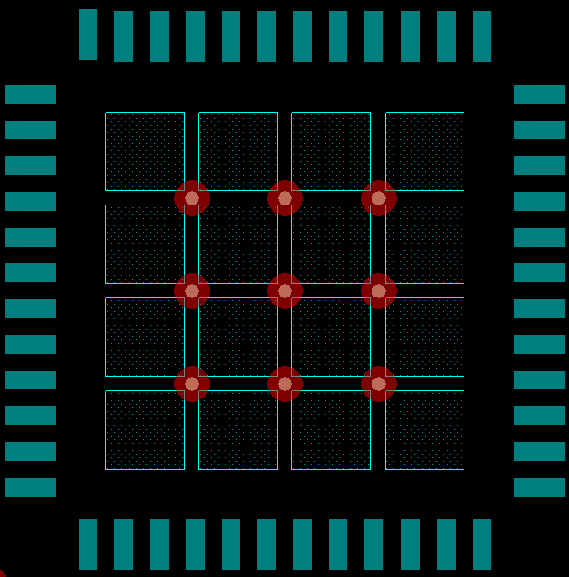
Stencil parameters such as aperture area ratio and the fabrication process have a significant impact on paste deposition. Inspection of the stencil prior to placement of the WQFN package is highly recommended to improve board assembly yields. If the via and aperture openings are not carefully monitored, the solder may flow unevenly through the DAP. Stencil parameters for aperture opening and via locations are shown below:
 Figure 41. No Pullback WQFN, Single Row Reference Diagram
 Table 13. No Pullback WQFN Stencil Aperture Summary for DS90UB914A-Q1
| DEVICE | PIN COUNT | MKT DWG | PCB I/O PAD SIZE (mm) | PCB PITCH (mm) | PCB DAP SIZE(mm) | STENCIL I/O APERTURE (mm) | STENCIL DAP APERTURE (mm) | NUMBER OF DAP APERTURE OPENINGS | GAP BETWEEN DAP APERTURE (Dim A mm) |
|---|---|---|---|---|---|---|---|---|---|
| DS90UB914A-Q1 | 48 | RHS | 0.25 x 0.6 | 0.5 | 5.1 x 5.1 | 0.25 x 0.7 | 1.1 x 1.1 | 16 | 0.2 |
 Figure 42. 48-Pin WQFN Stencil Example of Via and Opening Placement
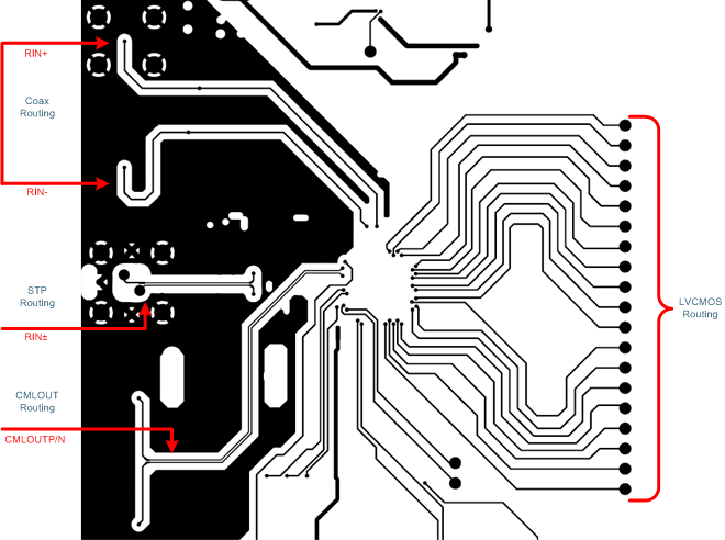
 The following PCB layout examples are derived from the layout design of the DS90UB914A-Q1 Evaluation Module (see DS90UB913A-CXEVM and DS90UB914A-CXEVM User’s Guide (SNLU135)). These graphics and additional layout description are used to demonstrate both proper routing and proper solder techniques when designing in this Deserializer.
