ZHCSEY3D April 2016 – October 2019 DS90UB914A-Q1
PRODUCTION DATA.
- 1 特性
- 2 应用
- 3 说明
- 4 修订历史记录
- 5 Device Comparison Table
- 6 Pin Configuration and Functions
-
7 Specifications
- 7.1 Absolute Maximum Ratings
- 7.2 ESD Ratings
- 7.3 Recommended Operating Conditions
- 7.4 Thermal Information
- 7.5 Electrical Characteristics
- 7.6 AC Timing Specifications (SCL, SDA) - I2C-Compatible
- 7.7 Bidirectional Control Bus DC Timing Specifications (SCL, SDA) - I2C-Compatible
- 7.8 Deserializer Switching Characteristics
- 7.9 Typical Characteristics
- 8 Parameter Measurement Information
-
9 Detailed Description
- 9.1 Overview
- 9.2 Functional Block Diagram
- 9.3
Feature Description
- 9.3.1 Serial Frame Format
- 9.3.2 Line Rate Calculations for the DS90UB913A/914A
- 9.3.3 Deserializer Multiplexer Input
- 9.3.4 Error Detection
- 9.3.5 Synchronizing Multiple Cameras
- 9.3.6 General-Purpose I/O (GPIO) Descriptions
- 9.3.7 LVCMOS VDDIO Option
- 9.3.8 EMI Reduction
- 9.3.9 Pixel Clock Edge Select (TRFB / RRFB)
- 9.3.10 Power Down
- 9.4
Device Functional Modes
- 9.4.1 DS90UB913A/914A Operation With External Oscillator as Reference Clock
- 9.4.2 DS90UB913A/914A Operation With Pixel Clock From Imager as Reference Clock
- 9.4.3 MODE Pin on Deserializer
- 9.4.4 Clock-Data Recovery Status Flag (LOCK), Output Enable (OEN) and Output State Select (OSS_SEL)
- 9.4.5 Built-In Self Test
- 9.4.6 BIST Configuration and Status
- 9.4.7 Sample BIST Sequence
- 9.5 Programming
- 9.6 Register Maps
- 10Application and Implementation
- 11Power Supply Recommendations
- 12Layout
- 13器件和文档支持
- 14机械、封装和可订购信息
10.1.2 Power-Up Requirements and PDB Pin
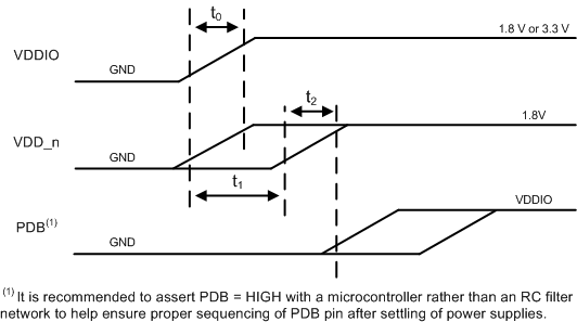
The PDB pin on the device must be ramped after the VDDIO and VDD_n supplies have reached their required operating voltage levels. It is recommended to assert PDB = HIGH with a control signal from a microcontroller to help ensure proper sequencing of the PDB pin after settling of the power supplies. If a microcontroller is not available, an RC filter network can be used on the PDB pin as an alternative method for asserting the PDB signal. Please refer to Power Down for device operation when powered down.
Common applications will tie the VDDIO and VDD_n supplies to the same power source of 1.8 V typically. This is an acceptable method for ramping the VDDIO and VDD_n supplies. The main constraint here is that the VDD_n supply does not lead in ramping before the VDDIO system supply. This is noted in Figure 28 with the requirement of t1≥ 0. VDDIO should reach the expected operating voltage earlier than VDD_n or at the same time.
Table 8. Power-Up Sequencing Constraints for DS90UB914A-Q1
If the FPD-Link system is not initialized in the correct sequence, the DS90UB914A-Q1 may need to be reset with signal present at the input to the Deserializer to optimize the link:
- Toggle the PDB power down reset pin, or:
- Perform Digital Reset 1 writing register 0x01[1] = 1 over I2C. It resets the entire digital block except registers in the 914A. This is a self-clearing register bit.
For the case of the loss of lock from cable when disconnecting and re-connecting FPD-Link cable, it is recommended to perform either PDB reset or digital reset via I2C when lock drops.
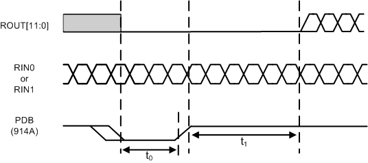
 Figure 29. Suggested Timing of PDB RESET for DS90UB914A-Q1 Deserializer
 Table 9. PDB RESET Timing Constraints for DS90UB914A-Q1
| PARAMETER | TEST CONDITIONS | MIN | TYP | MAX | UNIT | |
|---|---|---|---|---|---|---|
| t0 | PDB minimum LOW pulse width | 10% of falling edge to 10% of rising edge | 2 | 5 | ms | |
| t1 | Data Lock Time | 90% of rising edge | 15 | 22 | ms | |
Table 10. PDB to I2C Delay Requirements
| PARAMETER | MIN | TYP | MAX | UNIT | |
|---|---|---|---|---|---|
| t1 | PDB to I2C Ready | 2 | ms | ||

