ZHCSEY3D April 2016 – October 2019 DS90UB914A-Q1
PRODUCTION DATA.
- 1 特性
- 2 应用
- 3 说明
- 4 修订历史记录
- 5 Device Comparison Table
- 6 Pin Configuration and Functions
-
7 Specifications
- 7.1 Absolute Maximum Ratings
- 7.2 ESD Ratings
- 7.3 Recommended Operating Conditions
- 7.4 Thermal Information
- 7.5 Electrical Characteristics
- 7.6 AC Timing Specifications (SCL, SDA) - I2C-Compatible
- 7.7 Bidirectional Control Bus DC Timing Specifications (SCL, SDA) - I2C-Compatible
- 7.8 Deserializer Switching Characteristics
- 7.9 Typical Characteristics
- 8 Parameter Measurement Information
-
9 Detailed Description
- 9.1 Overview
- 9.2 Functional Block Diagram
- 9.3
Feature Description
- 9.3.1 Serial Frame Format
- 9.3.2 Line Rate Calculations for the DS90UB913A/914A
- 9.3.3 Deserializer Multiplexer Input
- 9.3.4 Error Detection
- 9.3.5 Synchronizing Multiple Cameras
- 9.3.6 General-Purpose I/O (GPIO) Descriptions
- 9.3.7 LVCMOS VDDIO Option
- 9.3.8 EMI Reduction
- 9.3.9 Pixel Clock Edge Select (TRFB / RRFB)
- 9.3.10 Power Down
- 9.4
Device Functional Modes
- 9.4.1 DS90UB913A/914A Operation With External Oscillator as Reference Clock
- 9.4.2 DS90UB913A/914A Operation With Pixel Clock From Imager as Reference Clock
- 9.4.3 MODE Pin on Deserializer
- 9.4.4 Clock-Data Recovery Status Flag (LOCK), Output Enable (OEN) and Output State Select (OSS_SEL)
- 9.4.5 Built-In Self Test
- 9.4.6 BIST Configuration and Status
- 9.4.7 Sample BIST Sequence
- 9.5 Programming
- 9.6 Register Maps
- 10Application and Implementation
- 11Power Supply Recommendations
- 12Layout
- 13器件和文档支持
- 14机械、封装和可订购信息
9.5.6 Multiple Device Addressing
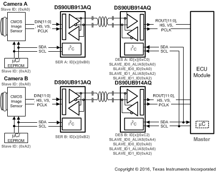
Some applications require multiple camera devices with the same fixed address to be accessed on the same I2C bus. The DS90UB914A provides slave ID matching/aliasing to generate different target slave addresses when connecting more than two identical devices together on the same bus. This allows the slave devices to be independently addressed. Each device connected to the bus is addressable through a unique ID by programming of the Slave alias register on Deserializer. This will remap the Slave alias address to the target SLAVE_ID address; up to 1 ID Alias is supported when slaves are attached to the DS90UB914A deserializer The ECU Controller must keep track of the list of I2C peripherals in order to properly address the target device.
See Figure 27 for an example of this function.
- ECU is the I2C master and has an I2C master interface
- The I2C interfaces in DES A and DES B are both slave interfaces
- The I2C protocol is bridged from DES A to SER A and from DES B to SER B
- The I2C interfaces in SER A and SER B are both master interfaces
If master controller transmits I2C slave 0xA0, DES A (address 0xC0), with pass through enabled, will forward the transaction to remote Camera A. If the controller transmits slave address 0xA4, the DES B 0xC2 will recognize that 0xA4 is mapped to 0xA0 and will be transmitted to the remote Camera B. If controller sends command to address 0xA6, the DES B (address 0xC2), with pass through enabled, will forward the transaction to slave device 0xA2.
 Figure 27. Multiple Device Addressing