ZHCSIS3C September   2018  – April 2024 DP83869HM

PRODUCTION DATA  

  1.   1
  2. 特性
  3. 应用
  4. 说明
  5. Device Comparison
  6. Pin Configuration and Functions
  7. Specifications
    1. 6.1 Absolute Maximum Ratings
    2. 6.2 ESD Ratings
    3. 6.3 Recommended Operating Conditions
    4. 6.4 Thermal Information
    5. 6.5 Electrical Characteristics
    6. 6.6 Timing Requirements
    7. 6.7 Timing Diagrams
    8. 6.8 Typical Characteristics
  8. Detailed Description
    1. 7.1 Overview
    2. 7.2 Functional Block Diagram
    3. 7.3 Feature Description
      1. 7.3.1  WoL (Wake-on-LAN) Packet Detection
        1. 7.3.1.1 Magic Packet Structure
        2. 7.3.1.2 Wake-on-LAN Configuration and Status
      2. 7.3.2  Start of Frame Detect for IEEE 1588 Time Stamp
        1. 7.3.2.1 SFD Latency Variation and Determinism
          1. 7.3.2.1.1 1000Mb SFD Variation in Master Mode
          2. 7.3.2.1.2 1000Mb SFD Variation in Slave Mode
          3. 7.3.2.1.3 100-Mb SFD Variation
      3. 7.3.3  Clock Output
      4. 7.3.4  Loopback Mode
        1. 7.3.4.1 Near-End Loopback
          1. 7.3.4.1.1 MII Loopback
          2. 7.3.4.1.2 PCS Loopback
          3. 7.3.4.1.3 Digital Loopback
          4. 7.3.4.1.4 Analog Loopback
          5. 7.3.4.1.5 External Loopback
          6. 7.3.4.1.6 Far-End (Reverse) Loopback
        2.       37
      5. 7.3.5  BIST Configuration
      6. 7.3.6  Interrupt
      7. 7.3.7  Power-Saving Modes
        1. 7.3.7.1 IEEE Power Down
        2. 7.3.7.2 Active Sleep
        3. 7.3.7.3 Passive Sleep
      8. 7.3.8  Mirror Mode
      9. 7.3.9  Speed Optimization
      10. 7.3.10 Cable Diagnostics
        1. 7.3.10.1 TDR
      11. 7.3.11 Fast Link Drop
      12. 7.3.12 Jumbo Frames
    4. 7.4 Device Functional Modes
      1. 7.4.1  Copper Ethernet
        1. 7.4.1.1 1000BASE-T
        2. 7.4.1.2 100BASE-TX
        3. 7.4.1.3 10BASE-Te
      2. 7.4.2  Fiber Ethernet
        1. 7.4.2.1 1000BASE-X
        2. 7.4.2.2 100BASE-FX
      3. 7.4.3  Serial GMII (SGMII)
      4. 7.4.4  Reduced GMII (RGMII)
        1. 7.4.4.1 1000Mbps Mode Operation
        2. 7.4.4.2 1000Mbps Mode Timing
        3. 7.4.4.3 10 and 100Mbps Mode
      5. 7.4.5  Media Independent Interface (MII)
      6. 7.4.6  Bridge Modes
        1. 7.4.6.1 RGMII-to-SGMII Mode
        2. 7.4.6.2 SGMII-to-RGMII Mode
        3.       67
      7. 7.4.7  Media Convertor Mode
      8. 7.4.8  Register Configuration for Operational Modes
        1. 7.4.8.1 RGMII-to-Copper Ethernet Mode
        2. 7.4.8.2 RGMII-to-1000Base-X Mode
        3. 7.4.8.3 RGMII-to-100Base-FX Mode
        4. 7.4.8.4 RGMII-to-SGMII Bridge Mode
        5. 7.4.8.5 1000M Media Convertor Mode
        6. 7.4.8.6 100M Media Convertor Mode
        7. 7.4.8.7 SGMII-to-Copper Ethernet Mode
      9. 7.4.9  Serial Management Interface
        1. 7.4.9.1 Extended Register Space Access
          1. 7.4.9.1.1 Read (No Post Increment) Operation
          2. 7.4.9.1.2 Write (No Post Increment) Operation
      10. 7.4.10 Auto-Negotiation
        1. 7.4.10.1 Speed and Duplex Selection - Priority Resolution
        2. 7.4.10.2 Master and Slave Resolution
        3. 7.4.10.3 Pause and Asymmetrical Pause Resolution
        4. 7.4.10.4 Next Page Support
        5. 7.4.10.5 Parallel Detection
        6. 7.4.10.6 Restart Auto-Negotiation
        7. 7.4.10.7 Enabling Auto-Negotiation Through Software
        8. 7.4.10.8 Auto-Negotiation Complete Time
        9. 7.4.10.9 Auto-MDIX Resolution
    5. 7.5 Programming
      1. 7.5.1 Strap Configuration
        1. 7.5.1.1 Straps for PHY Address
        2. 7.5.1.2 Strap for DP83869HM Functional Mode Selection
        3. 7.5.1.3 LED Default Configuration Based on Device Mode
        4. 7.5.1.4 Straps for RGMII/SGMII to Copper
        5. 7.5.1.5 Straps for RGMII to 1000Base-X
        6. 7.5.1.6 Straps for RGMII to 100Base-FX
        7. 7.5.1.7 Straps for Bridge Mode (SGMII-RGMII)
        8. 7.5.1.8 Straps for 100M Media Convertor
        9. 7.5.1.9 Straps for 1000M Media Convertor
      2. 7.5.2 LED Configuration
      3. 7.5.3 Reset Operation
        1. 7.5.3.1 Hardware Reset
        2. 7.5.3.2 IEEE Software Reset
        3. 7.5.3.3 Global Software Reset
        4. 7.5.3.4 Global Software Restart
    6. 7.6 Register Maps
      1. 7.6.1 DP83869 Registers
  9. Application and Implementation
    1. 8.1 Application Information
    2. 8.2 Typical Applications
      1. 8.2.1 Copper Ethernet Typical Application
        1. 8.2.1.1 Design Requirements
        2. 8.2.1.2 Detailed Design Procedure
          1. 8.2.1.2.1 Clock Input
            1. 8.2.1.2.1.1 Crystal Recommendations
            2. 8.2.1.2.1.2 External Clock Source Recommendation
          2. 8.2.1.2.2 Magnetics Requirements
            1. 8.2.1.2.2.1 Magnetics Connection
        3. 8.2.1.3 Application Curves
      2. 8.2.2 Fiber Ethernet Typical Ethernet
        1. 8.2.2.1 Design Requirements
        2. 8.2.2.2 Detailed Design Procedure
          1. 8.2.2.2.1 Transceiver Connections
        3. 8.2.2.3 Application Curves
    3. 8.3 Power Supply Recommendations
      1. 8.3.1 Two-Supply Configuration
      2. 8.3.2 Three-Supply Configuration
    4. 8.4 Layout
      1. 8.4.1 Layout Guidelines
        1. 8.4.1.1 Signal Traces
          1. 8.4.1.1.1 MAC Interface Layout Guidelines
            1. 8.4.1.1.1.1 SGMII Layout Guidelines
            2. 8.4.1.1.1.2 RGMII Layout Guidelines
          2. 8.4.1.1.2 MDI Layout Guidelines
        2. 8.4.1.2 Return Path
        3. 8.4.1.3 Transformer Layout
        4. 8.4.1.4 Metal Pour
        5. 8.4.1.5 PCB Layer Stacking
      2. 8.4.2 Layout Example
  10. Device and Documentation Support
    1. 9.1 Documentation Support
      1. 9.1.1 Related Documentation
    2. 9.2 Receiving Notification of Documentation Updates
    3. 9.3 支持资源
    4. 9.4 Trademarks
    5. 9.5 静电放电警告
    6. 9.6 术语表
  11. 10Revision History
  12. 11Mechanical, Packaging, and Orderable Information

封装选项

机械数据 (封装 | 引脚)
散热焊盘机械数据 (封装 | 引脚)
订购信息

Fast Link Drop

The DP83869HM includes advanced link-down capabilities that support various real-time applications. The link down mechanism is configurable and includes enhanced modes that allow extremely fast reaction times to link drops.
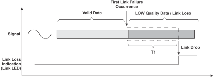
DP83869HM Fast Link Drop MechanismFigure 7-5 Fast Link Drop Mechanism

As described in Figure 7-5, the link loss mechanism is based on a time window search period in which the signal behavior is monitored. The T1 window is set by default to reduce typical link drops to less than 1ms in 100M and 0.5ms in 1000M mode.

The DP83869HM supports enhanced modes that shorten the window called Fast Link Down mode. In this mode, the T1 window is shortened significantly, in most cases less than 10μs. In this period of time, there are several criteria allowed to generate link loss event and drop the link:

  1. Loss of descrambler sync
  2. Receive errors
  3. MLT3 errors
  4. Mean Squared Error (MSE)
  5. Energy loss

The Fast Link Down functionality allows the use of each of these options separately or in any combination. Note that because this mode enables extremely quick reaction time, it is more exposed to temporary bad link quality scenarios.