ZHCSE88A October 2015 – February 2023 DLPA3005
PRODUCTION DATA
- 1 特性
- 2 应用
- 3 说明
- 4 Revision History
- 5 Pin Configuration and Functions
- 6 Specifications
-
7 Detailed Description
- 7.1 Overview
- 7.2 Functional Block Description
- 7.3
Feature Description
- 7.3.1 Supply and Monitoring
- 7.3.2 Illumination
- 7.3.3 External Power FET Selection
- 7.3.4 DMD Supplies
- 7.3.5 Buck Converters
- 7.3.6 Auxiliary LDOs
- 7.3.7 Measurement System
- 7.4 Device Functional Modes
- 7.5 Programming
- 7.6 Register Maps
- 8 Application and Implementation
- 9 Power Supply Recommendations
- 10Layout
- 11Device and Documentation Support
- 12Mechanical, Packaging, and Orderable Information
7.3.2.1 Programmable Gain Block
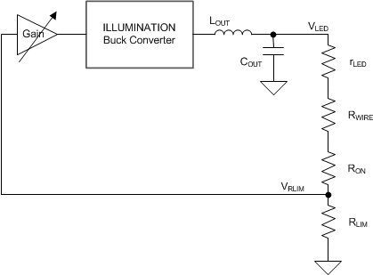
The current through the LEDs is determined by a digital number stored in the respective SWx_IDAC(x) registers, 0x03h to 0x08h. These registers determine the LED current which is measured through the sense resistor RLIM. The voltage across RLIM is compared with the current setting from the IDAC registers and the loop regulates the current to its set value.
 Figure 7-3 Programmable Gain Block in the Illumination Control Loop
When current is flowing through an LED, a forward voltage is built up over the LED. The LED also represents a (low) differential resistance which is part of the load circuit for VLED. Together with the wire resistance (RWIRE) and the RON resistance of the FET switch a voltage divider is created with RLIM that is a factor in the loop gain of the ILED control. Under normal conditions, the loop is able to produce a well regulated LED current up to 16 Amps.
Since this voltage divider is part of the control loop, care must be taken while designing the system.
When, for instance, two LEDs in series are connected, or when a relatively high wiring resistance is present in the loop, the loop gain will reduce due to the extra attenuation caused by the increased series resistances of rLED + RWIRE +RON. As a result, the loop response time lowers. To compensate for this increased attenuation, the loop gain can be increased by selecting a higher gain for the programmable gain block. The gain increase can be set through register ILLUM_BW_BCx.
Under normal circumstances the default gain setting (00h) is sufficient. In case of a series connection of two LEDs setting 01h or 02h might suffice.
As discussed previously, wiring resistance also impacts the control-loop performance. It is advisable to prevent unnecessary large wire length in the loop. Keeping wiring resistance as low as possible is good for efficiency reasons. In case wiring resistance still impacts the response time of the loop, an appropriate setting of the gain block can be selected. The same goes for connector resistance and PCB tracks. Note that every milliohm (mΩ) counts. These precautions help to ensure the proper functioning of the ILED current loop.