ZHCSE88A October   2015  – February 2023 DLPA3005

PRODUCTION DATA  

  1. 特性
  2. 应用
  3. 说明
  4. Revision History
  5. Pin Configuration and Functions
  6. Specifications
    1. 6.1 Absolute Maximum Ratings
    2. 6.2 ESD Ratings
    3. 6.3 Recommended Operating Conditions
    4. 6.4 Thermal Information
    5. 6.5 Electrical Characteristics
    6. 6.6 SPI Timing Parameters
  7. Detailed Description
    1. 7.1 Overview
    2. 7.2 Functional Block Description
    3. 7.3 Feature Description
      1. 7.3.1 Supply and Monitoring
        1. 7.3.1.1 Supply
        2. 7.3.1.2 Monitoring
          1. 7.3.1.2.1 Block Faults
          2. 7.3.1.2.2 Auto LED Turn Off Functionality
          3. 7.3.1.2.3 Thermal Protection
      2. 7.3.2 Illumination
        1. 7.3.2.1 Programmable Gain Block
        2. 7.3.2.2 LDO Illumination
        3. 7.3.2.3 Illumination Driver A
        4. 7.3.2.4 RGB Strobe Decoder
          1. 7.3.2.4.1 Break Before Make (BBM)
          2. 7.3.2.4.2 Openloop Voltage
          3. 7.3.2.4.3 Transient Current Limit
        5. 7.3.2.5 Illumination Monitoring
          1. 7.3.2.5.1 Power Good
          2. 7.3.2.5.2 Ratio Metric Overvoltage Protection
        6. 7.3.2.6 Illumination Driver plus Power FETs Efficiency
      3. 7.3.3 External Power FET Selection
        1. 7.3.3.1 Threshold Voltage
        2. 7.3.3.2 Gate Charge and Gate Timing
        3. 7.3.3.3 RDS(ON)
      4. 7.3.4 DMD Supplies
        1. 7.3.4.1 LDO DMD
        2. 7.3.4.2 DMD HV Regulator
        3. 7.3.4.3 DMD/DLPC Buck Converters
        4. 7.3.4.4 DMD Monitoring
          1. 7.3.4.4.1 Power Good
          2. 7.3.4.4.2 Overvoltage Fault
      5. 7.3.5 Buck Converters
        1. 7.3.5.1 LDO Bucks
        2. 7.3.5.2 General Purpose Buck Converter
        3. 7.3.5.3 Buck Converter Monitoring
          1. 7.3.5.3.1 Power Good
          2. 7.3.5.3.2 Overvoltage Fault
        4. 7.3.5.4 Buck Converter Efficiency
      6. 7.3.6 Auxiliary LDOs
      7. 7.3.7 Measurement System
    4. 7.4 Device Functional Modes
    5. 7.5 Programming
      1. 7.5.1 SPI
      2. 7.5.2 Interrupt
      3. 7.5.3 Fast-Shutdown in Case of Fault
      4. 7.5.4 Protected Registers
    6. 7.6 Register Maps
  8. Application and Implementation
    1. 8.1 Application Information
    2. 8.2 Typical Application
      1. 8.2.1 Design Requirements
      2. 8.2.2 Detailed Design Procedure
        1. 8.2.2.1 Component Selection for General-Purpose Buck Converters
      3. 8.2.3 Application Curve
    3. 8.3 System Example With DLPA3005 Internal Block Diagram
  9. Power Supply Recommendations
    1. 9.1 Power-Up and Power-Down Timing
  10. 10Layout
    1. 10.1 Layout Guidelines
      1. 10.1.1 SPI Connections
      2. 10.1.2 RLIM Routing
      3. 10.1.3 LED Connection
    2. 10.2 Layout Example
    3. 10.3 Thermal Considerations
  11. 11Device and Documentation Support
    1. 11.1 Device Support
      1. 11.1.1 Device Nomenclature
    2. 11.2 第三方产品免责声明
    3. 11.3 Related Links
    4. 11.4 接收文档更新通知
    5. 11.5 支持资源
    6. 11.6 Trademarks
    7. 11.7 静电放电警告
    8. 11.8 术语表
  12. 12Mechanical, Packaging, and Orderable Information
    1. 12.1 Package Option Addendum

封装选项

机械数据 (封装 | 引脚)
散热焊盘机械数据 (封装 | 引脚)
订购信息

Supply

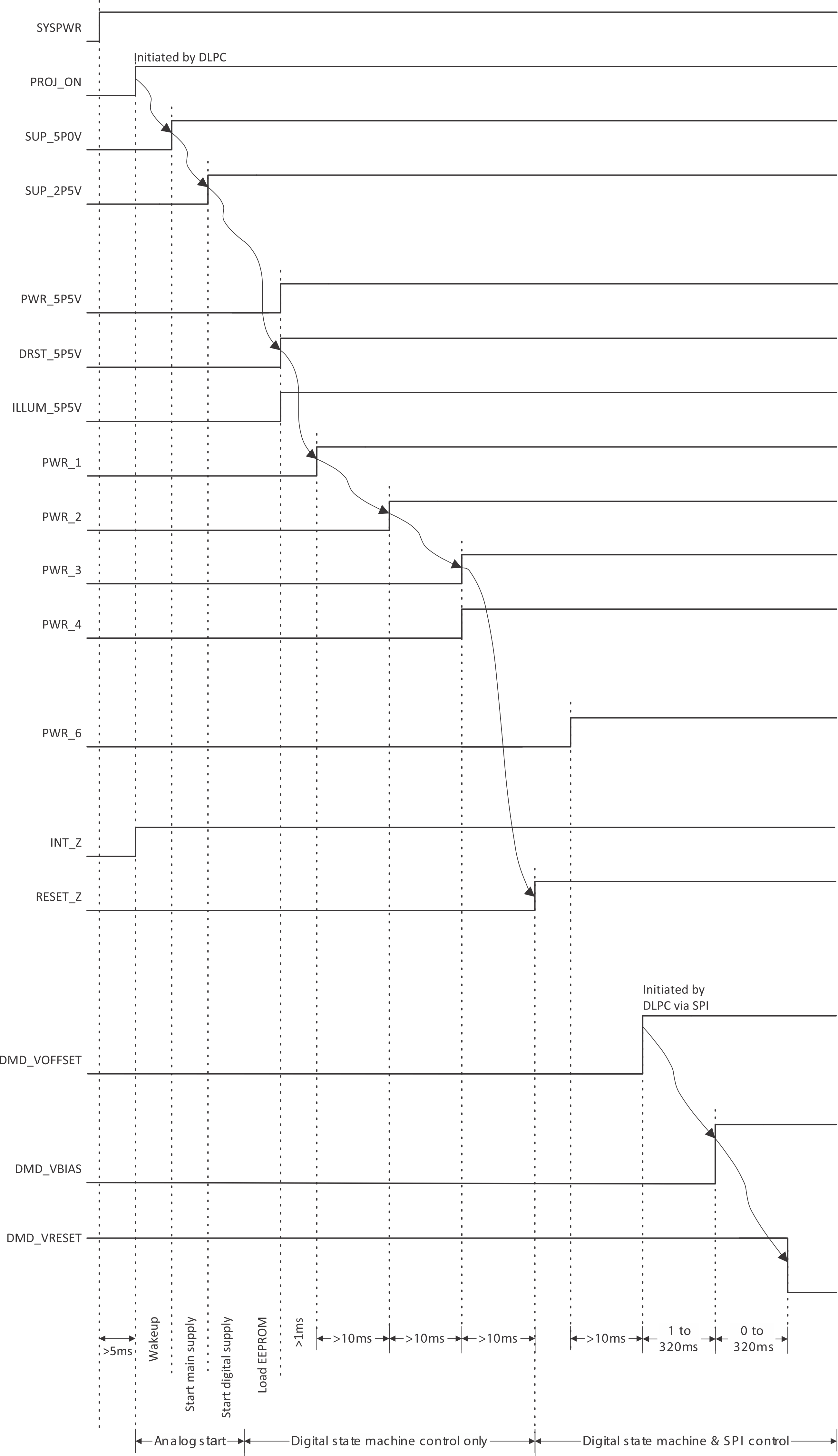
SYSPWR is the main supply of the DLPA3005. It can range from 6 V to 20 V, where the typical is 12 V. At power-up, several (internal) power supplies are started one after the other in order to make the system work correctly (#DLPS0412076). A sequential startup ensures that all the different blocks start in a certain order and prevent excessive startup currents. The main control to start the DLPA3005 is the control pin PROJ_ON. Once set high the basic analog circuitry is started that is needed to operate the digital and SPI interface. This circuitry is supplied by two LDO regulators that generate 2.5 V (SUP_2P5V) and 5 V (SUP_5P0V). These regulator voltages are for internal use only and should not be loaded by an external application. The output capacitors of those LDOs should be 2.2 µF for the 2.5-V LDO, and 4.7 µF for the 5-V LDO, pin 91 and 92 respectively. Once these are up the digital core is started, and the DLPA3005 Digital State Machine (DSM) takes over.

Subsequently, the 5.5-V LDOs for various blocks are started: PWR_5V5V, DRST_5P5V and ILLUM_5P5V. Next, the buck converters and DMD LDOs are started (PWR_1 to PWR_4). The DLPA3005 is now awake and ready to be controlled by the DLPC (indicated by RESET_Z going high).

The general purpose buck converter (PWR_6) can be started (if used) as well as the regulator that supplies the DMD. The DMD regulator generates the timing critical VOFFSET, VBIAS, and VRESET supplies.
GUID-9C5F7C03-5466-4162-87D9-C41E1EFAE3C7-low.gif
  1. Arrows indicate sequence of events automatically controlled by digital state machine. Other events are initiated under SPI control.
  2. SUP_5P0V and SUP_2P5V rise to a precharge level with SYSPWR, and reach the full level potential after PROJ_ON is pulled high.
Figure 7-1 Powerup Timing