ZHCSE88A October   2015  – February 2023 DLPA3005

PRODUCTION DATA  

  1. 特性
  2. 应用
  3. 说明
  4. Revision History
  5. Pin Configuration and Functions
  6. Specifications
    1. 6.1 Absolute Maximum Ratings
    2. 6.2 ESD Ratings
    3. 6.3 Recommended Operating Conditions
    4. 6.4 Thermal Information
    5. 6.5 Electrical Characteristics
    6. 6.6 SPI Timing Parameters
  7. Detailed Description
    1. 7.1 Overview
    2. 7.2 Functional Block Description
    3. 7.3 Feature Description
      1. 7.3.1 Supply and Monitoring
        1. 7.3.1.1 Supply
        2. 7.3.1.2 Monitoring
          1. 7.3.1.2.1 Block Faults
          2. 7.3.1.2.2 Auto LED Turn Off Functionality
          3. 7.3.1.2.3 Thermal Protection
      2. 7.3.2 Illumination
        1. 7.3.2.1 Programmable Gain Block
        2. 7.3.2.2 LDO Illumination
        3. 7.3.2.3 Illumination Driver A
        4. 7.3.2.4 RGB Strobe Decoder
          1. 7.3.2.4.1 Break Before Make (BBM)
          2. 7.3.2.4.2 Openloop Voltage
          3. 7.3.2.4.3 Transient Current Limit
        5. 7.3.2.5 Illumination Monitoring
          1. 7.3.2.5.1 Power Good
          2. 7.3.2.5.2 Ratio Metric Overvoltage Protection
        6. 7.3.2.6 Illumination Driver plus Power FETs Efficiency
      3. 7.3.3 External Power FET Selection
        1. 7.3.3.1 Threshold Voltage
        2. 7.3.3.2 Gate Charge and Gate Timing
        3. 7.3.3.3 RDS(ON)
      4. 7.3.4 DMD Supplies
        1. 7.3.4.1 LDO DMD
        2. 7.3.4.2 DMD HV Regulator
        3. 7.3.4.3 DMD/DLPC Buck Converters
        4. 7.3.4.4 DMD Monitoring
          1. 7.3.4.4.1 Power Good
          2. 7.3.4.4.2 Overvoltage Fault
      5. 7.3.5 Buck Converters
        1. 7.3.5.1 LDO Bucks
        2. 7.3.5.2 General Purpose Buck Converter
        3. 7.3.5.3 Buck Converter Monitoring
          1. 7.3.5.3.1 Power Good
          2. 7.3.5.3.2 Overvoltage Fault
        4. 7.3.5.4 Buck Converter Efficiency
      6. 7.3.6 Auxiliary LDOs
      7. 7.3.7 Measurement System
    4. 7.4 Device Functional Modes
    5. 7.5 Programming
      1. 7.5.1 SPI
      2. 7.5.2 Interrupt
      3. 7.5.3 Fast-Shutdown in Case of Fault
      4. 7.5.4 Protected Registers
    6. 7.6 Register Maps
  8. Application and Implementation
    1. 8.1 Application Information
    2. 8.2 Typical Application
      1. 8.2.1 Design Requirements
      2. 8.2.2 Detailed Design Procedure
        1. 8.2.2.1 Component Selection for General-Purpose Buck Converters
      3. 8.2.3 Application Curve
    3. 8.3 System Example With DLPA3005 Internal Block Diagram
  9. Power Supply Recommendations
    1. 9.1 Power-Up and Power-Down Timing
  10. 10Layout
    1. 10.1 Layout Guidelines
      1. 10.1.1 SPI Connections
      2. 10.1.2 RLIM Routing
      3. 10.1.3 LED Connection
    2. 10.2 Layout Example
    3. 10.3 Thermal Considerations
  11. 11Device and Documentation Support
    1. 11.1 Device Support
      1. 11.1.1 Device Nomenclature
    2. 11.2 第三方产品免责声明
    3. 11.3 Related Links
    4. 11.4 接收文档更新通知
    5. 11.5 支持资源
    6. 11.6 Trademarks
    7. 11.7 静电放电警告
    8. 11.8 术语表
  12. 12Mechanical, Packaging, and Orderable Information
    1. 12.1 Package Option Addendum

封装选项

机械数据 (封装 | 引脚)
散热焊盘机械数据 (封装 | 引脚)
订购信息

RDS(ON)

The selection of the FET relative to its drain-source on-resistance, RDS(ON), has two aspects. First, for the high-side FET of the illumination buck-converter, the RDS(ON) is a factor in the overcurrent detection. Second, for the other four FETs, the power dissipation drives the choice of the FETs RDS(ON).

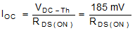
To detect an overcurrent situation, the DLPA3005 measures the drain-source voltage drop of the high-side FET when turned on. The overcurrent detection circuit triggers, and switches off the high-side FET, when the threshold VDC-Th = 185 mV (typical) is reached. Therefore, the actual current, IOC, at which this overcurrent detection triggers, is given by:

Equation 6. GUID-0FF290B6-C05F-4C23-9DAD-B8666091F6D3-low.gif

Note that the RDS(ON) should be taken from the FET data sheet at high-temperature , that is, at overcurrent the FETs will likely by hot.

For example, the CSD17510Q5A NexFET has an RDS(ON) of 7 mΩ at 125°C. Using this FET will result in an overcurrent level of 26 A. This FET would be a good choice for a 16 A application.

For the low-side FET and the three LED selection FETs the RDS(ON) selection is mainly governed by the power dissipation due to conduction losses. The power dissipated in these FETs is given by:

Equation 7. GUID-12A65081-4A5A-41FF-BCC1-C5B437378C2A-low.gif

In which IDS is the current running through the respective FET. The lower the RDS(ON), the lower is the dissipation.

For example, the CSD17501Q5A has RDS(ON)= 3 mΩ. For a drain-source current of 16 A with a duty cycle of 25% (assuming the FET is used as LED selection switch), the dissipation is about 0.2 W in this FET.