ZHCU763 March 2021
- 说明
- 资源
- 特性
- 应用
- 5
- 1System Description
-
2System Overview
- 2.1 Block Diagram
- 2.2
Design Considerations
- 2.2.1 Multichannel SSR with Independent Isolation Between SSR Channels
- 2.2.2 Design Challenge With Single Isolation
- 2.2.3 Multichannel SSR Drive With Single Isolation Multichannel Digital Isolator
- 2.2.4 Need of High-Impedance Voltage Translator
- 2.2.5 Design to Minimize Cross-Coupling and MOSFET Gate Pick up Due to Other SSR Switching
- 2.2.6 Schematic: Design of Gate-Drive Circuit
- 2.2.7 Schematic: Digital Isolator Circuit
- 2.2.8 Schematic: 3.3 V to 10V_ISO, 5V_ISO Power Supply
- 2.3 Highlighted Products
- 3Hardware, Software, Testing Requirements, and Test Results
- 4Design and Documentation Support
- 5About the Author
2.2.6 Schematic: Design of Gate-Drive Circuit
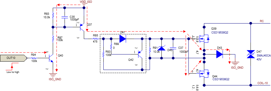
Figure 2-9 shows the gate-drive circuit of one channel of SSR and the SSR turn on gate current path. OUT10 is the relay on and off signal at the secondary side of the digital isolator. When OUT10 goes from logic low (0 V) to logic high (5 V), the NPN transistor Q40 turns on. For multichannel implementation, the NPN transistor can be replaced by a low-side switch array device, the TPL7407LA. The TPL7407LA integrates seven low-side NMOS switches and can be used to replace the NPN transistors of seven SSR channels. Turning on the NPN transistor Q40 will bias the PNP transistor Q37 through the resistors R83 and R87 and enable sufficient base current to turn on Q37. Once Q37 turns on, the SSR MOSFET gate-to-source will be charged to VGD_ISO through Q37, R85 (gate resistor), D41, and D43. The components in the dotted box including D41, Q42, R89, and R93 are not required in most of the use cases, if a slow turn off is enough for the application (a few tens of micro seconds to hundreds of micro-seconds).
The peak gate current is to be designed by adjusting the biasing of the PNP transistor. In the reference design, the bias resistors used are R83 = 10 kΩ and R87 = 100 kΩ. The value is designed in such a way that Q37 gets sufficient bias voltage when VGD is greater than 6.5 V. With R83 = 10 kΩ, and R87 = 100 kΩ, the base current of Q37 is approximately 10 µA as per simulation results.
With VGD_ISO = 8.5 V and R87 = 100 kΩ, IB = 10 µA. The saturation collector current of Q2 (same as the peak gate current) can be calculated as, IC = Igate_peak = DC current gain of Q37 × IB.
Assuming DC current gain = 200 (from the PNP transistor data sheet), IC = 2 mA.
The Zener diode D45 acts as a clamp for overvoltage protection at the gate-to-source of the MOSFET.
 Figure 2-9 Gate Driver Circuit for the SSR
MOSFETs and the Turn on Gate Current Path
Figure 2-9 Gate Driver Circuit for the SSR
MOSFETs and the Turn on Gate Current PathThe gate-drive circuit can experience overvoltage in the case of mis-wiring at the side of the power relay coil and 24 VAC transformer. Considering a mis-wiring, where the 24 VAC is connected to the RC terminal of SSR-1, and the RC terminal of SSR-2 is left unconnected. The relay coils are connected from both SSR MOSFET lower terminals (COIL-1 and COIL-2) to the common wire (C-wire). In this use case, if both SSR are kept ON, then the full AC voltage will appear across the blocking diode (diode connected between common source of MOSFET to ISO_GND) and the peak value of that voltage can be 41 V (corresponding to 24 VAC +20%). In this case, the possible overvoltage at the gate-source of MOSFET in any SSR channel needs to be avoided in design by adding Zener diode across the gate and source terminal of SSR MOSFET.
Approximate peak voltage across PNP transistor = 41 V, assuming VGD_ISO = 8.5 V, and VAC (peak) = 41 V.
The peak power loss in Q37 = 41 V × 2 mA = 82 mW, the average power loss across Q2 will be lower.
The peak current through gate-source resistance R91 (when the Zener diode clamps to Vz = 12 V) can be calculated as, IR91 = 12 V / R91 = 1.2 mA.
The peak current in the Zener diode = Igate_peak – current through R91 = 0.8 mA.
The peak power loss in the gate clamp Zener diode = 12 × 0.8 mA = 9.6 mW.
A 250 mW–500 mW Zener is a good option in design.
The previously-mentioned power loss happens only during mis-wiring and during normal working condition the Zener diode will not be carrying any current and the PNP transistor power loss also will be much lower. The user has the option to reduce the peak gate current further by increasing the base bias resistors of PNP transistor Q37, at the expense of slow turn on and turn off of the SSR MOSFETs. While reducing the peak gate current, make sure that the gate-to-source resistance R91 value is increased accordingly to ensure enough gate voltage at the MOSFET gate.
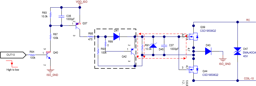
Figure 2-10 shows the turn off gate drive path. When OUT10 goes low, Q40 turns off, Q37 turns off and the MOSFET gate discharges through R91 and Q42.
 Figure 2-10 Gate Driver Circuit for the SSR MOSFETs and the Turn off Gate Current Path