TIDUF05 August   2022


  1.   Description
  2.   Resources
  3.   Features
  4.   Applications
  5.   5
  6. 1System Description
    1. 1.1 Key System Specifications
  7. 2System Overview
    1. 2.1 Block Diagram
    2. 2.2 Design Considerations
      1. 2.2.1 PCB and Form Factor
      2. 2.2.2 Power Supply Design
        1. 2.2.2.1 POC Filter
        2. 2.2.2.2 Power Supply Considerations
          1. 2.2.2.2.1 Choosing External Components
          2. 2.2.2.2.2 Choosing the Buck 1 Inductor
          3. 2.2.2.2.3 Choosing the Buck 2 and Buck 3 Inductors
        3. 2.2.2.3 Functional Safety
    3. 2.3 Highlighted Products
      1. 2.3.1 AR0820 Imager
      2. 2.3.2 DS90UB953-Q1
      3. 2.3.3 TPS650330-Q1
    4. 2.4 System Design Theory
  8. 3Hardware, Testing Requirements, and Test Results
    1. 3.1 Hardware Requirements
      1. 3.1.1 Hardware Setup
      2. 3.1.2 FPD-Link III I2C Initialization
      3. 3.1.3 AR0820 Initialization
    2. 3.2 Test Setup
      1. 3.2.1 Power Supplies Start Up
      2. 3.2.2 Camera Functionality
    3. 3.3 Test Results
      1. 3.3.1 Power Supplies Start-Up
      2. 3.3.2 Power Supply Start-Up—1.8-V Rail and PDB
      3. 3.3.3 Power Supply Voltage Ripple
      4. 3.3.4 Power Supply Load Currents
      5. 3.3.5 Video Output
  9. 4Design and Documentation Support
    1. 4.1 Design Files
      1. 4.1.1 Schematics
      2. 4.1.2 Bill of Materials
      3. 4.1.3 PCB Layout Recommendations
        1. 4.1.3.1 Layout Prints
        2. 4.1.3.2 PMIC Layout Recommendations
        3. 4.1.3.3 Serializer Layout Recommendations
        4. 4.1.3.4 Imager Layout Recommendations
        5. 4.1.3.5 PCB Layer Stackup Recommendations
      4. 4.1.4 Altium Project
      5. 4.1.5 Gerber Files
  10. 5Documentation Support
  11. 6Support Resources
  12. 7Trademarks

PCB and Form Factor

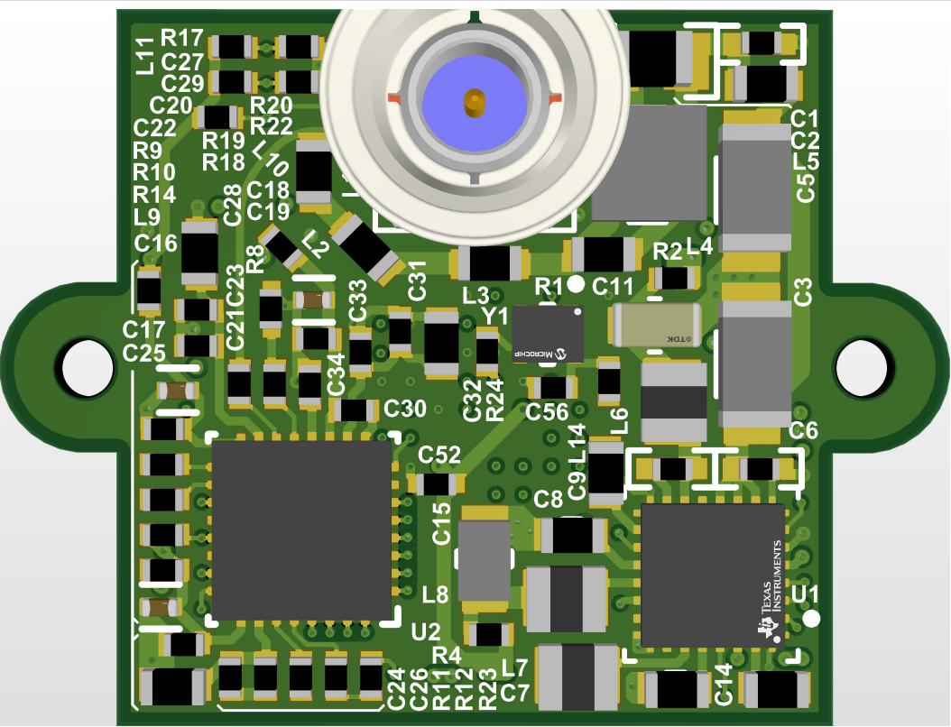
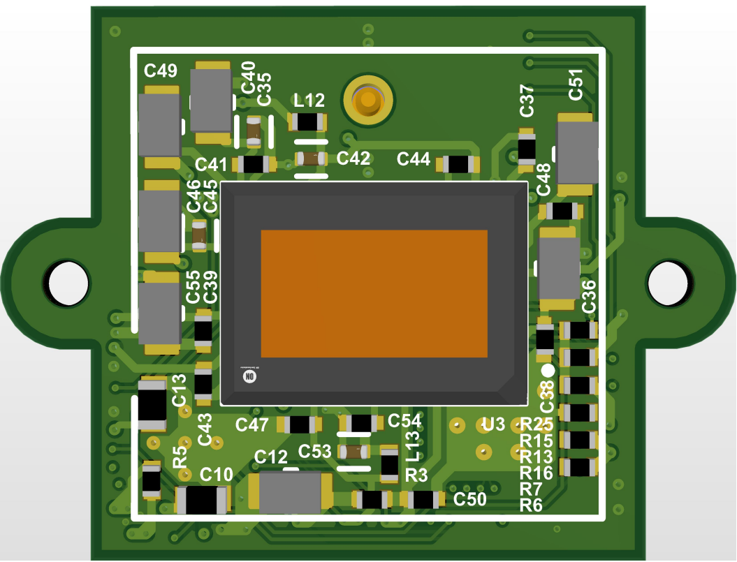
This reference design is not intended to fit any particular form factor; however, the goal of the design is to showcase a solution with minimal PCB area and compact design. The area of the board roughly equates to a dimension of 20 mm × 20 mm. The area near the board edge in Figure 2-2 is reserved for attaching the optics housing that holds the lens.
GUID-20220421-SS0I-T0R2-SWWM-RFHLHXVL83QN-low.pngFigure 2-2 3-D PCB Top Layer
GUID-20220421-SS0I-BZ93-KTLC-WKGDHGK17JQ1-low.pngFigure 2-3 3-D PCB Bottom Layer